ED-7306_E.pdf - 第4页
JEITA ED-7306 - 2 - b) For the packages whose stand off height is 0.1 mm or less, such as FLGA, the measuring area is the substrate surface except certain e dge margin (See Fig. 3 , dimension L). The width of this margin…
JEITA ED-7306
- 1 -
Standard of Japan Electronics and Information Technology Industries Association
Measurement methods of package warpage at elevated temperature
and the maximum permissible warpage
Foreword
This standard was prepared by the Subcommittee on Integrated Circuit packages, Technical
Standardization Committee on Semiconductor Device Packages (TSC), Japan Electronics and Information
Technology Industries Association.
The increased reflow temperatures associated with lead-free reflow processes are prone to cause larger
warpages of packages and PWB, which have resulted in the detrimental effect on the yield of the board
level assembly. Under such circumstances, the Subcommittee started deliberations to standardize the
measurement method of package warpage at elevated temperature on Jun. 2005. After the deliberations
and agreements on the measurement methods and the criteria of the maximum permissible package
warpage, this standard was approved by TSC in Mar. 2007.
1. Scope
This standard stipulates the package warpage criteria and the package warpage measurement methods at
elevated temperature for BGA, FBGA, and FLGA
2. Normative references
The following referenced documents are indispensable for the application of this document. For dated
references, only the edition cited applies. For undated references, the latest edition of the referenced
document applies.
JEITA EDR-7315 Design guide for semiconductor packages, Ball Grid Array Package (BGA)
JEITA EDR-7316 Design guide for semiconductor packages, Fine-pitch Ball Grid Array and
Fine-pitch Land Grid Array (FBGA/FLGA)
JEITA ED-4701/300 Environmental and endurance test methods for semiconductor devices
TEST METHOD 301B
Resistance to soldering heat for surface mounting devices (SMD)
JEITA ED-7304 Measuring method for Package Dimensions of Ball Grid Array
3. Terms and definitions
For the purposes of this document, the following terms and definitions apply.
3.1 Measuring zone
The area to be measured to determine the package warpage.
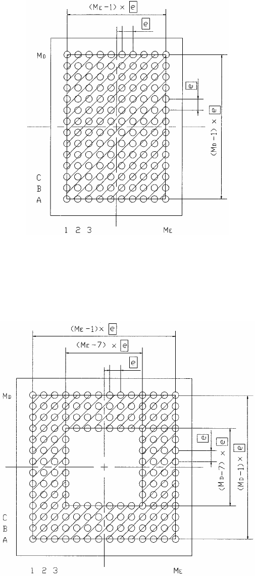
a) For the packages whose standoff height is more than 0.1 mm, such as BGA and FBGA, the measuring
zone is the area where terminals are located. This area is bordered by the lines connecting the centers
of the outermost neighboring solder balls (See Fig. 1 and Fig. 2). If there are thermal balls at the
package center, their area is also considered as a part of measuring zones.
JEITA ED-7306
- 2 -
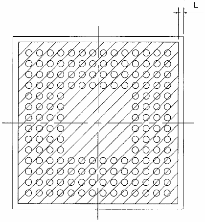
b) For the packages whose standoff height is 0.1 mm or less, such as FLGA, the measuring area is the
substrate surface except certain edge margin (See Fig. 3, dimension L). The width of this margin L
depends on the capability of each measuring instrument (0.2 mm recommended).
NOTE: The hatched area indicates the measuring zone.
Fig. 1 Measuring zone of BGA and FBGA in full grid layout
Fig. 2 Measuring zone of BGA and FBGA perimeter layout with 4 rows and 4 columns
JEITA ED-7306
- 3 -
NOTE: The edge margin L indicates the exempt area from measurement to avoid measurement
noise depending on the instrument capability. Recommended edge margin L=0.2 mm.
Fig. 3 Measuring zone of FLGA perimeter layout with 4 rows and 4 columns
3.2 Convex warpage
Arched top surface (not interconnect side) of package being mounted on PWB. The sign of the convex
warpage is defined as plus.
3.3 Concave warpage
Inward-curving top surface (not interconnect side) of package being mounted on PWB. The sign of the
concave warpage is defined as minus.
3.4 Package warpage sign
Plus or minus sign of package warpage determined by the sign of the sum of the largest positive
displacement and the largest negative displacement of the package profile on both measurement zone
diagonals. These diagonals are regarded as base lines connecting the outermost opposite corners of the
measuring zone. The sign of the package warpage is defined as the sign of:
(AB
MAX
+AB
MIN
+CD
MAX
+CD
MIN
).
AB
MAX
is the largest positive displacement and AB
MIN
is the largest negative displacement of the package
profile on the diagonal AB; (The sign of AB
MAX
is plus and AB
MIN
is zero in Fig. 4.)
CD
MAX
is the largest positive displacement and CD
MIN
is the largest negative displacement of the package
profile on the diagonal CD; (The sign of CD
MAX
is plus and that of CD
MIN
is minus in Fig. 4.)
The concave or convex impression of the package warpage can differ from the above defined sign, in
critical case.