ED-7306_E.pdf - 第9页
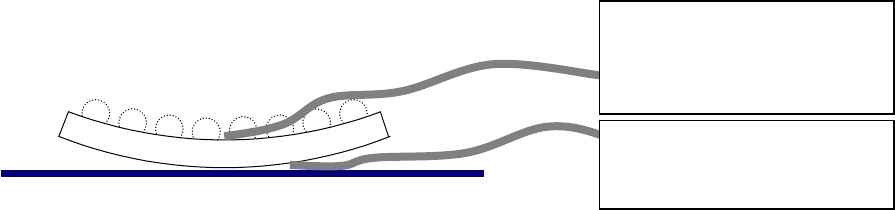
JEITA ED-7306 - 7 - 5.3.2 Laser reflection method Solder balls shall be removed wh en the solder ball pitch is not larg e enough for laser beam to measure the warpage on the subst rate surface. Samples are pla ced on the…
JEITA ED-7306
- 6 -
5.2.2 The temperatures for measurements are
- room temperature,
- melting point,
- peak temperature,
- solidification point, and
- room temperature after cool down.
The melting point and the solidification point are 220°C for Sn-3.0Ag-0.5Cu solder as a reference. Other
solder composites may take different temperatures. The peak temperature basically conforms to the
package classifications specified in TEST METHOD 301B, JEITA ED-4701/300, but to be exact, it shall
follow the supplier’s recommended max temperature.
5.2.3 It is recommended that a thermocouple of gauge 30 (φ0.25 mm) or flat tip type be used.
5.2.4 The thermocouple is attached on the center of the package body using either thermally conductive
epoxy or heat-resistant polyimide tape. When polyimide tape is used, thermally conductive sheet shall
be applied between the thermocouple bead and the package surface to enhance thermal conductivity
as a thermal interface material.
5.2.5 When a measuring instrument is being set up, the temperature of the molded side of the package
facing a heater is also measured. The temperature difference from the substrate surface shall
preferably be less than 10°C by adjusting the heating mechanism and the temperature profile.
Fig. 6 Thermocouple placement
5.3 Measurement method
5.3.1 Shadow moiré method
Solder balls shall be removed prior to the measurement on the substrate surface. Measurements are
conducted by placing the grating (low CTE glass with transparent and opaque stripes) parallel to the
sample. Then, the projection of light beam at an angle of approximately 45° through the grating produces
the stripe pattern on the sample. Observation of the stripe pattern through the grating results in the moiré
fringe pattern (geometric interference pattern). Image processing and the analysis of the patterns provide
the displacement from planarity over the substrate surface. The instrument is capable of setting the
measuring zone and measuring the warpage at elevated temperatures including the peak temperature.
Heater side
Package
Thermocouple on the substrate
side for temperature profile
control (warpage measurement
side)
Thermocouple on the molded
side for one time adjustment of
the temperature difference
JEITA ED-7306
- 7 -
5.3.2 Laser reflection method
Solder balls shall be removed when the solder ball pitch is not large enough for laser beam to measure the
warpage on the substrate surface. Samples are placed on the measurement table. The displacement from
the flatness is measured by the laser displacement sensor. The warpage is generally measured by
scanning the laser beam over the terminal lands or between balls throughout the measuring zone. The grid
pitch of the measurement points is preferably less than the solder ball pitch. The instrument is capable of
setting the measuring zone and measuring the warpage at elevated temperatures including the peak
temperature.
5.3.3 Data analysis (Data table, Diagonal scan graph, 3D plot graph)
The magnitude of the warpage is obtained from the data table of the measurements or 3D plot graph
(warpage distribution diagram over the measuring zone). Then the sign of the warpage (warpage direction)
is determined from the diagonal scan graph and precedes the value.
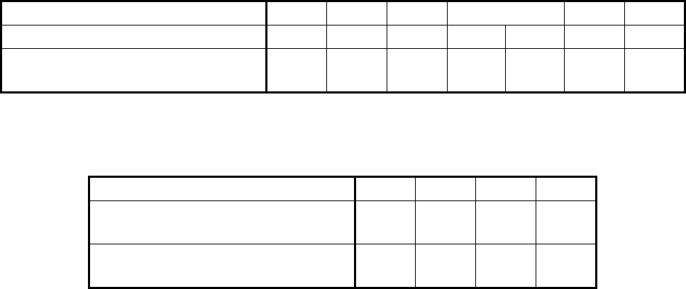
6. Maximum permissible package warpage at elevated temperature
The criteria of the maximum permissible package warpages for BGA and FBGA are specified in Table 1,
and those for FLGA are specified in Table 2.
Table 1 Maximum permissible package warpages for BGA and FBGA
Unit: mm
Solder ball pitch 0.4 0.5 0.65 0.8 1.0 1.27
Condition of ball height 0.20 0.25 0.33 0.35 0.40 0.50 0.60
Maximum permissible package warpage
(Absolute value)
0.10 0.11 0.14 0.17 0.17 0.22 0.25
Table 2 Maximum permissible package warpages for FLGA
Unit: mm
Land pitch 0.4 0.5 0.65 0.8
Condition of thickness of molten solder
paste
0.08 0.10 0.11 0.13
Maximum permissible package warpage
(Absolute value)
0.08 0.10 0.11 0.13
JEITA ED-7306
- 8 -
7. Recommended datasheet for the package warpage
7.1 Measurement temperatures for data sheet
Typical measurement temperatures for datasheet are room temperature, melting point, peak temperature,
solidification point, and room temperature after cooling.
7.2 Datasheet
Datasheet is composed of
- temperature dependency of the package warpage (See Fig. 7),
- surface topography at each temperature in 3D plots (optional). (If the sign of warpage is opposite,
explanation is required; See Fig. 8),
- diagonal profile of the package at each temperature (optional). (If the sign of warpage is opposite,
explanation is required; See Fig. 8),
- explanatory figure of the sign of the package warpage (optional), and
- temperature profile for measurement.
7.3 Example of datasheets
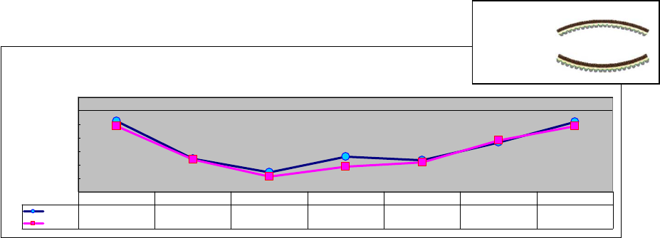
Fig. 7 Temperature dependency of the package warpage
Average warpage
for xxxx & yyyy
-70
-60
-50
-40
-30
-20
-10
0
Warpage(um)
xxxxAVG
-17.8 -46 -55.7 -44 -47 -33.8 -18.3
yyyy
AVG
-21.5 -46.2 -58.7 -51.8 -48.5 -32 -21.8
25C 150C 220C 260C 220C 150C 25C
+/
-
Sign
+
-
Warpage(µm)
0
-10
-20
-30
-40
-50
-60
-70
25°C 150°C 220°C 260°C 220°C 150°C 25°C