MV-9_Chapter 5. Teaching.pdf - 第105页
错误 ! 使用“开始” 选项卡将 제목 2 应用于要在此处显示的文字。 错误 ! 使用“开始”选项卡将 제목 2 应用 于要在此处显示的 文字。 . 5- 105 Luminance comparison [F igure 5-1 10 lumin a nce comp arison inspection result] Pixel co mp ariso n [Figure 5- 111 Luminan ce comparis…
MV-9 User Manual
5-104
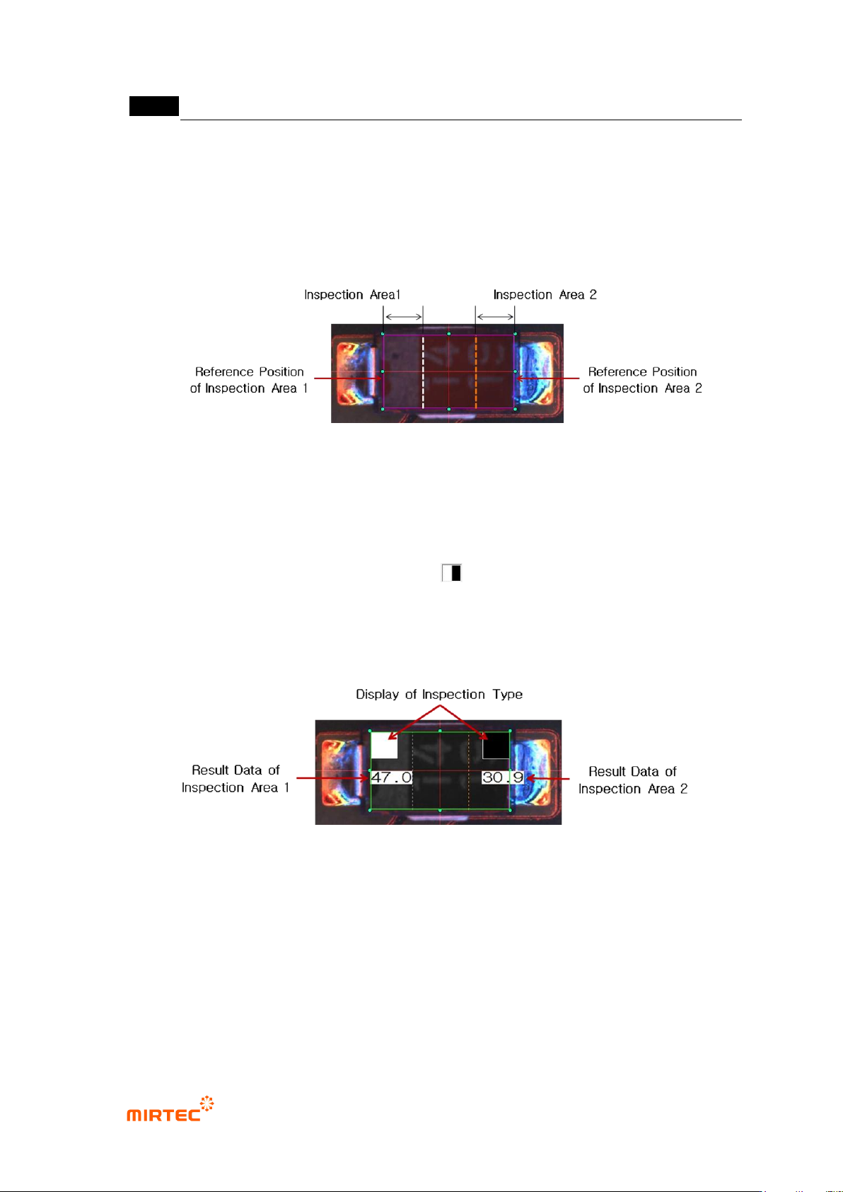
Width of each inspection area can be designated in electrode display area and
comparison target area.
White line is boundary line for inspection area 1, and yellow line is boundary line for
inspection area 2 during teaching. The left and top will be allotted as inspection
area 1, and right and bottom will be allotted as inspection area 2 based on based
on 0 degree during teaching, and they rotate together according to rotation angle.
[Figure 5-108 inspection area setting]
- Inspection criteria
Set difference of luminance between 2 areas or difference of pixel ratio. Sign of
inequality will be judged by inspection type.
For example, when inspection type is selected, judged as normal if inspection
criteria of inspection area 1 is higher than inspection area 2.
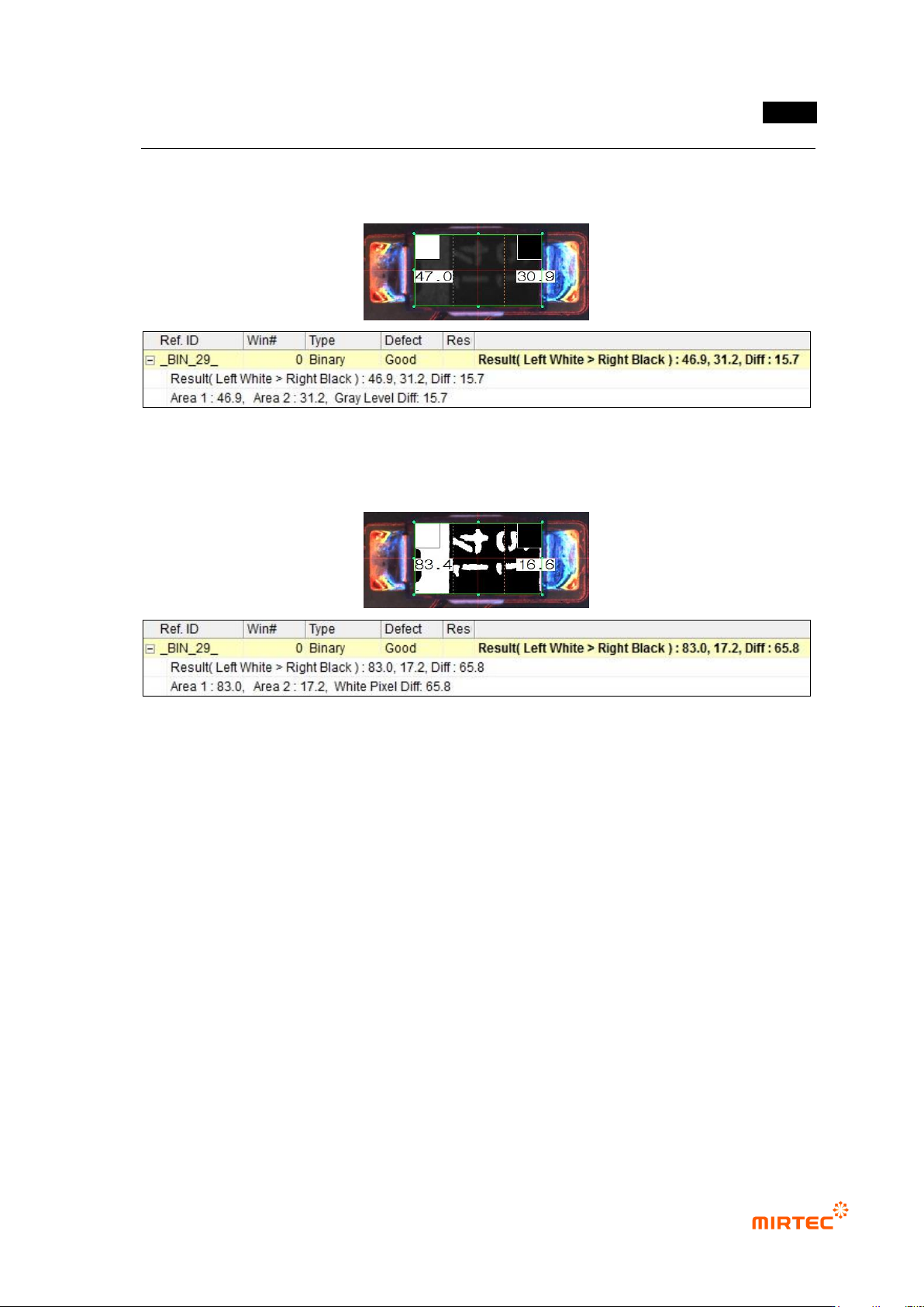
③ Inspection result in status screen
[Figure 5-109 Comparison inspection result display status (Trial inspection)]
- Result (Left White> Right Black): difference (Diff) between inspection result value 2 areas.
The left in brackets is white and the right is black, and calculation value in the left must be
above the right.
- Area 1, Area 2: average luminance or white pixel ratio of each area
- Gray Level Diff or White Pixel Diff: difference of average luminance of 2 areas or difference
of white pixel ratio
错误!使用“开始”选项卡将 제목 2 应用于要在此处显示的文字。错误!使用“开始”选项卡将 제목 2 应用
于要在此处显示的文字。 .
5-105
Luminance comparison
[Figure 5-110 luminance comparison inspection result]
Pixel comparison
[Figure 5-111 Luminance comparison inspection result]
MV-9 User Manual
5-106
5.3.6 IC/Bridge inspection window
- IC/Bridge inspection is an algorithm to detect defect that occurs at lead part of IC
component. judge whether there is bridge between lead and defect of soldering status of
each lead end. this system sets one inspection area to inspect various errors that occurs
at lead part of IC component to increase users‟ operational convenience and the system
has detailed adjustment items for inspection to raise inspection reliability.
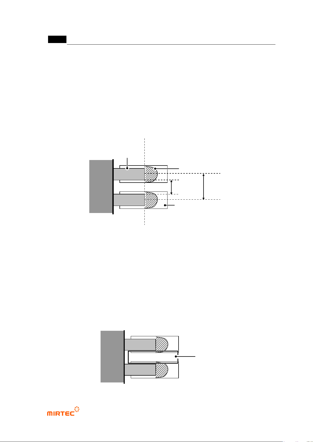
1) Definition of each area of IC lead
[Figure 5-112 IC lead part]
Bridge defect
- In case of normal (no defect), solder must exist only on pad area that fixes IC lead.
However, in case of a defect, solder on the pad pushed out into gap area between lead
and connect both lead. This is called as Bridge defect.
- To detect this defect, solder in gap area must be checked to inspect IC lead. Hence, judge
bridge defect by checking binarization of image from camera and distribution shape of
white pixel in gap area.
- this system conducts separate lead separation before inspection to increase bridge
inspection performance and use separate and Bridge inspection for separated gap area.
Inspection area
Lead end
Solder Fillet
Lead
Pitch
Gap
Pad