MV-9_Chapter 5. Teaching.pdf - 第175页
错误 ! 使用“开始” 选项卡将 제목 2 应用于要在此处显示的文字。 错误 ! 使用“开始”选项卡将 제목 2 应用 于要在此处显示的 文字。 . 5- 175 Set good/d ef ect j udgment cri teria for differenc e with ave rage va l ue of a ll l ead t i p position or difference w ith l ead t i p…
MV-9 User Manual
5-174
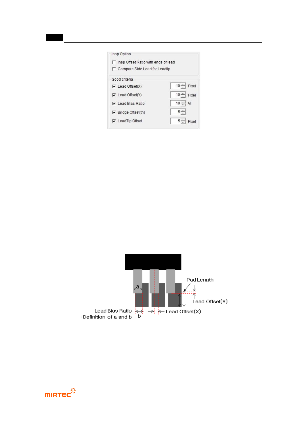
[Figure 5-210 inspection option and normal criteria]
Normal criteria
- Lead offset
This item is to inspect Shift of IC package.
Lead offset (X): set good/defect judgment criteria for distance between lead center
and pad center.
Lead offset (Y): set good/defect judgment criteria for degree of lead shift.
- Lead shift ratio
This item is for inspection for shift or lead bending of IC package. set lead shift
criteria. Lead shift ratio is defined by the ratio of overlapped area of lead and pad,
and calculate to (b / a) x100.
[Figure 5-211 pad inspection parameter screen]
- Bridge offset (angle)
This option will be activated if lead offset of normal criteria is checked.
Set angle offset criteria of Bridge.
- Lead tip offset
错误!使用“开始”选项卡将 제목 2 应用于要在此处显示的文字。错误!使用“开始”选项卡将 제목 2 应用
于要在此处显示的文字。 .
5-175
Set good/defect judgment criteria for difference with average value of all lead tip
position or difference with lead tip of adjacent lead (for side lead comparison
setting).
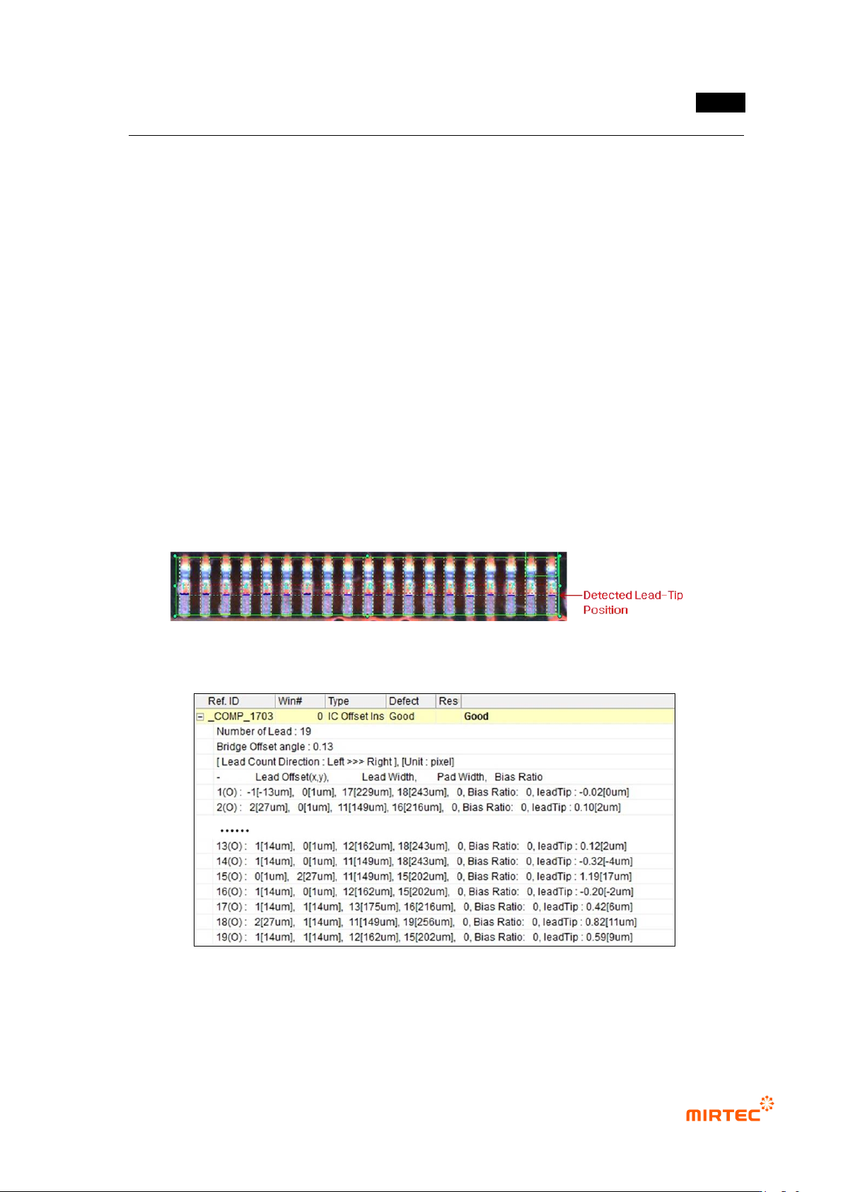
4) Inspection result in status screen
- Number of Lead: display number of lead.
- Bridge Offset Angle: angle of IC package calculated by using position of lead tip.
- Lead Count Direction [unit]: increase direction of lead No. Unit is the unit of displayed data.
- Lead Offset: difference between distance from pad end to lead tip and pad length (value
set on teaching tap).
- Lead Width: lead width detected in lead search range.
- Pad Width: pad width detected in pad search range.
- Bias Ratio: overlap ratio of pad and lead
- Lead Tip: lead tip difference (difference between average value and adjacent lead).
[Figure 5-212 IC offset inspection result image]
[Figure 5-213 IC offset inspection result screen]
MV-9 User Manual
5-176
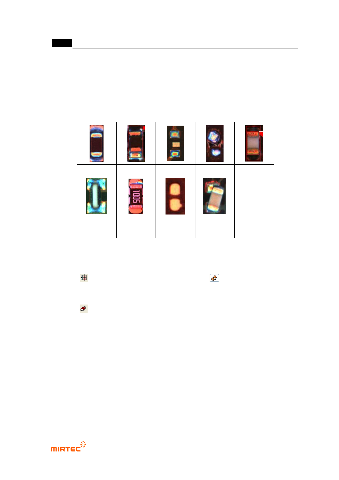
5.3.13 Chip color inspection
Chip color inspection is algorithm to detect defect that occurs in body area and soldering area of
chip component. use data that measured color component of solder with slope to inspect
soldering status. The figure below shows defect images.
normal
lifted
non-mounting
Manhattan
turnover
Tomb Stone
insufficient
solder
No solder
Tilt
[Figure 5-214 Chip defect types]
5) Teaching method
① Click button and draw mounting window. Select light and select R (Red) for
image type. image type is R of light of same angle with that of vertical light of the existing
white light, and B (Blue) is light of angle that is same with that of horizontal light.
② Click button, and draw window including both solder parts of chip.
③ Select both of 2 windows, and click [right button of a mouse → popup menu → adjust →
component center] to adjust the center of 2 windows.
④ For chip color inspection window, components must be grouped like those of mounting
window. Therefore, click [right button of a mouse → popup menu →‟Group component‟].
⑤ As shown in [Figure 5-159], group the components and select [mounting inspection type →
chip color].