MV-9_Chapter 5. Teaching.pdf - 第177页
错误 ! 使用“开始” 选项卡将 제목 2 应用于要在此处显示的文字。 错误 ! 使用“开始”选项卡将 제목 2 应用 于要在此处显示的 文字。 . 5- 177 mounting in spection window chip c olor ins pe ct ion – chip body window chip c olor ins pe ct ion – pad inspect ion w indo w [Figure 5- 2…
MV-9 User Manual
5-176
5.3.13 Chip color inspection
Chip color inspection is algorithm to detect defect that occurs in body area and soldering area of
chip component. use data that measured color component of solder with slope to inspect
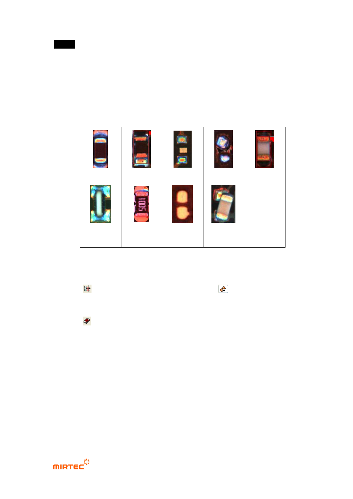
soldering status. The figure below shows defect images.
normal
lifted
non-mounting
Manhattan
turnover
Tomb Stone
insufficient
solder
No solder
Tilt
[Figure 5-214 Chip defect types]
5) Teaching method
① Click button and draw mounting window. Select light and select R (Red) for
image type. image type is R of light of same angle with that of vertical light of the existing
white light, and B (Blue) is light of angle that is same with that of horizontal light.
② Click button, and draw window including both solder parts of chip.
③ Select both of 2 windows, and click [right button of a mouse → popup menu → adjust →
component center] to adjust the center of 2 windows.
④ For chip color inspection window, components must be grouped like those of mounting
window. Therefore, click [right button of a mouse → popup menu →‟Group component‟].
⑤ As shown in [Figure 5-159], group the components and select [mounting inspection type →
chip color].
错误!使用“开始”选项卡将 제목 2 应用于要在此处显示的文字。错误!使用“开始”选项卡将 제목 2 应用
于要在此处显示的文字。 .
5-177
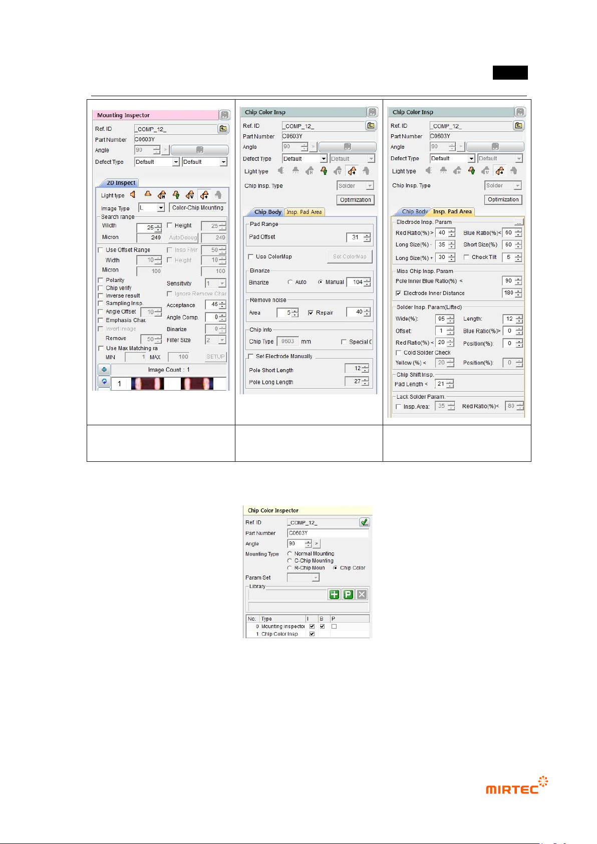
mounting inspection window
chip color inspection – chip body
window
chip color inspection – pad
inspection window
[Figure 5-215 mounting inspection and chip color inspection parameter]
[Figure 5-216 Selecting chip color after ‘Group component’]
MV-9 User Manual
5-178
[Figure 5-217 chip color inspection window]
6) Parameter of [chip color inspection] window
Optimization
After completing teaching, click optimization button. Chip type, chip body tap (electrode minor
axis length, electrode major axis length, pad offset, binarization) and pad inspection tap (size of
lifted inspection area, chip offset) information will be automatically calculated and allotted using
the result.
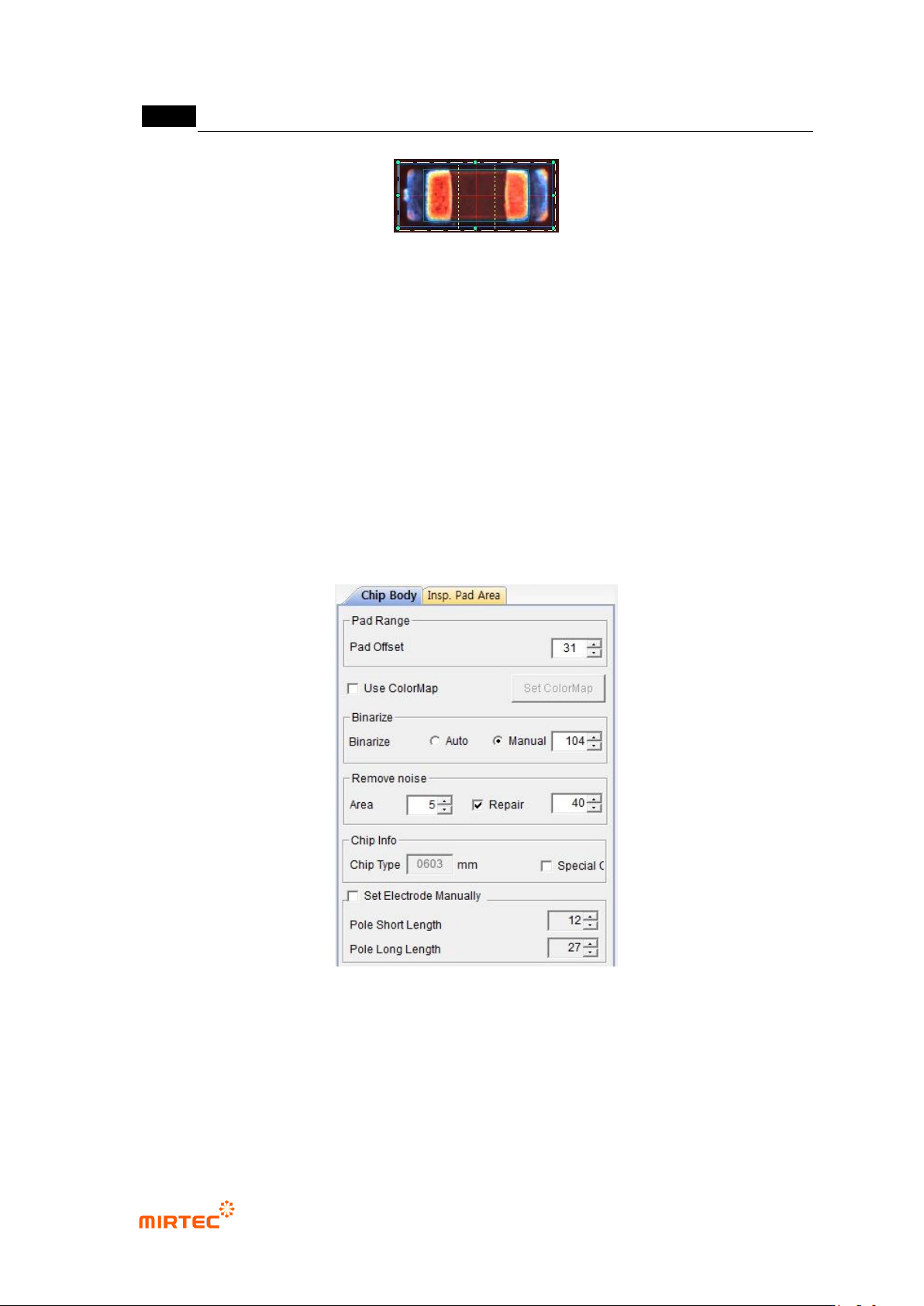
7) Parameter of [chip body] tap
[chip body] tap is to extract pad offset and electrode. This plays the role of calculating optimum
chip inspection parameter.
[Figure 5-218 parameter window of chip body tap]
Pad range
① Pad offset
- Set offset value as long as pad length at both ends in chip color inspection window.
designate range for electrode extraction and area to inspect non-mounting.