MV-9_Chapter 5. Teaching.pdf - 第179页
错误 ! 使用“开始” 选项卡将 제목 2 应用于要在此处显示的文字。 错误 ! 使用“开始”选项卡将 제목 2 应用 于要在此处显示的 文字。 . 5- 179 - If normal separation of electrode is not done because all par t of chip became one due to binarization or too high b inariza t i on va l…
MV-9 User Manual
5-178
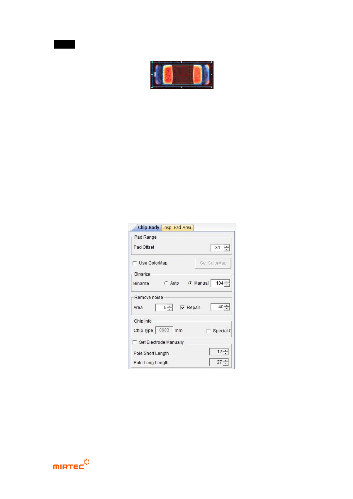
[Figure 5-217 chip color inspection window]
6) Parameter of [chip color inspection] window
Optimization
After completing teaching, click optimization button. Chip type, chip body tap (electrode minor
axis length, electrode major axis length, pad offset, binarization) and pad inspection tap (size of
lifted inspection area, chip offset) information will be automatically calculated and allotted using
the result.
7) Parameter of [chip body] tap
[chip body] tap is to extract pad offset and electrode. This plays the role of calculating optimum
chip inspection parameter.
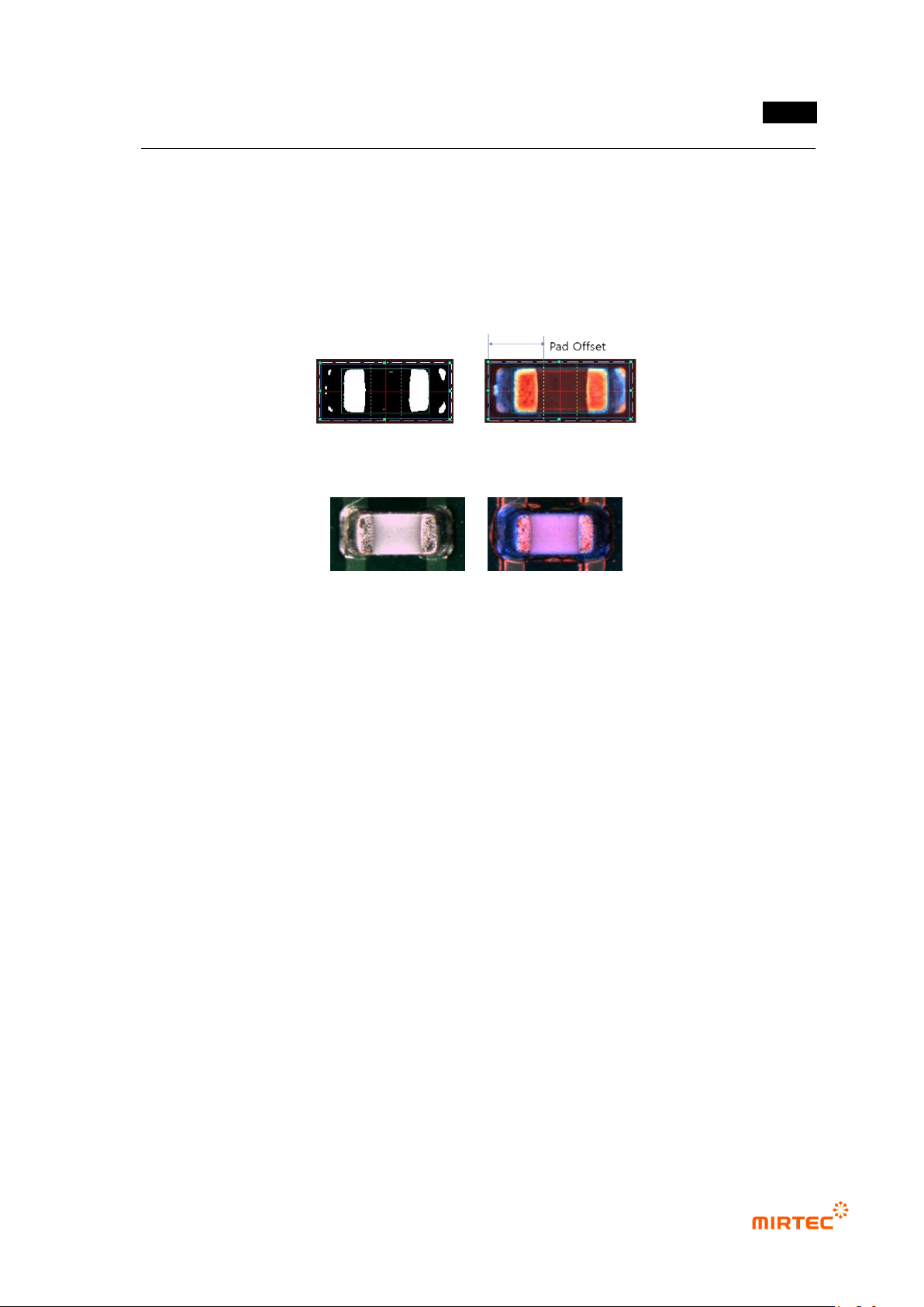
[Figure 5-218 parameter window of chip body tap]
Pad range
① Pad offset
- Set offset value as long as pad length at both ends in chip color inspection window.
designate range for electrode extraction and area to inspect non-mounting.
错误!使用“开始”选项卡将 제목 2 应用于要在此处显示的文字。错误!使用“开始”选项卡将 제목 2 应用
于要在此处显示的文字。 .
5-179
- If normal separation of electrode is not done because all part of chip became one due to
binarization or too high binarization value must be used for electrode separation, adjust
pad offset position close to chip electrode to limit electrode size.
- Sometimes, locate it close electrode to reduce false defect of non-mounting. However, if
window is warped, yellow dotted line will be set in electrode area. Hence, do not set it too
closely to electrode.
[Figure 5-219 pad offset definition]
(Horizontal image) (Color image)
[Figure 5-220 Example of chip of which electrode is not separated from chip body]
Binarization
- Click „optimize‟ button to conduct optimization after initial teaching, and check for good
separation of electrode in preview. If electrode and chip body is not separated, set proper
value for binarization boundary value for good separation of electrode and chip body part
checking preview.
- After adjusting binarization value, make sure to click optimization button to refresh chip
information (electrode size, electrode distance).
- Adjust parameter on chip body tap before optimization after teaching, and click
optimization button to ignore chip body parameter set by operator. Hence, make sure to
firstly conduct optimization before parameter adjustment after teaching.
Noise removal
① Area
- This is used to extract only electrode by removing white noise besides electrode. Enter
size of white noise to be removed in pixel unit.
② Electrode edit width
MV-9 User Manual
5-180
- This is to extract electrode only. Check at the button to remove body edge component and
to find electrode. At this point, width of edge to be removed is below certain ratio of
electrode width, remove it. The following is calculation formula of width ratio. As shown in
[Figure 5-164], Width_1 and Width_2 is the width of silk to be removed, Width_3 is the
width electrode.
100
Width_3
Width_2)(Width_1
(%)edit width electrode
[Figure 5-221 noise removal – definition of electrode edit width]
Chip Info
① Chip Type
- This will be automatically set in optimization stage, and judge and display chip model that
completed teaching using size of mounting window.
② Special chip
- If the body area of chip to be inspected is displayed in blue (In case of component of which
chip body is blue), check special chip, select color map-pad on [pad inspection] tap, and
then adjust color map to display chip body area in blue.
- In general, Manhattan and Tomb Stone of normal C chip is judged based on the fact that
body area is red. In case of normal R chip, judged based on the fact that body area is
black, and in case of chip color algorithm, judged based on blue ratio in chip body area.
Chip of which chip body is blue will be judged as defect under these judgment criteria.
Therefore, special chip setting is special condition to reduce false defect.
- In case of setting a special chip, if blue ratio in chip body area is lower than reference
value that is set inside (user change is impossible based on 1/3 of other area excluding
electrode on chip), judge as defect.
(Horizontal image) (Color image)
[Figure 5-222 Example of chip of which chip body area is blue]