MV-9_Chapter 5. Teaching.pdf - 第183页
错误 ! 使用“开始” 选项卡将 제목 2 应用于要在此处显示的文字。 错误 ! 使用“开始”选项卡将 제목 2 应用 于要在此处显示的 文字。 . 5- 183 - Color type co nsists of red , green , and blue. Select color to adjust area des i red to be binarized for each color . - In other words,…
MV-9 User Manual
5-182
electrode is 44 and calculated electrode minor axis length is 20 when optimization is
clicked, short size ratio will be calculated to 120%. If minor axis length of electrode is
changed to 23 to set this to max 100%, short size ratio will be reduced down to 91%.
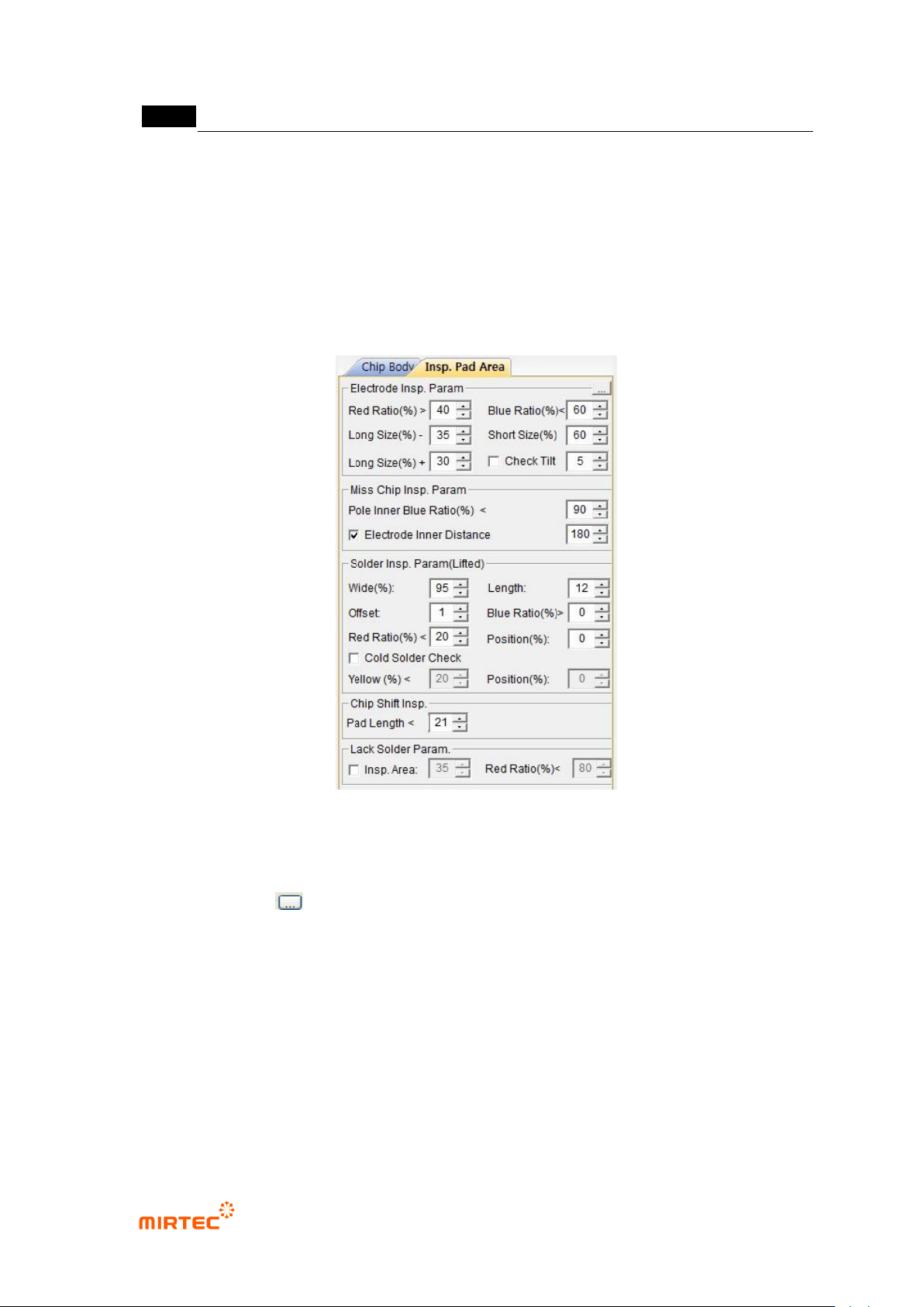
8) Parameter of [pad inspection] tap
- Pad inspection tap is to set criteria for good/defect judgment of chip.
[Figure 5-224 Parameter window of pad extraction tap]
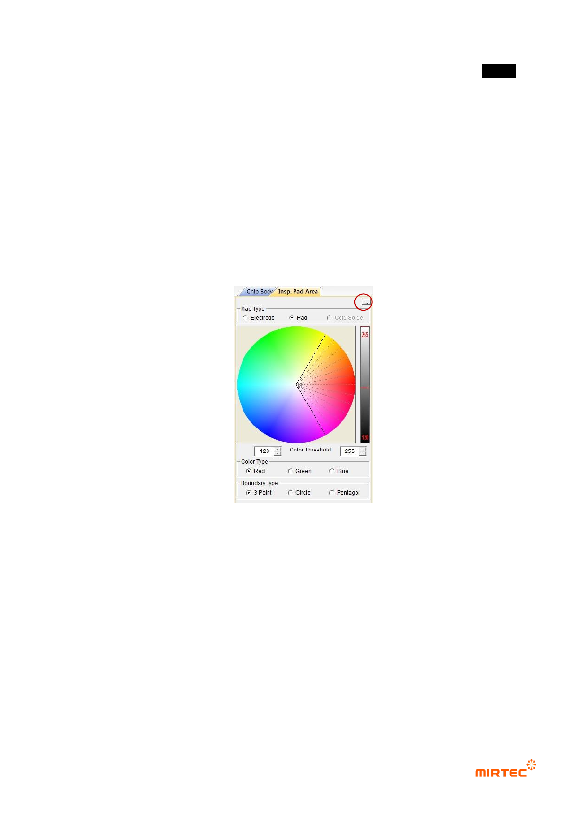
Adjusting color map for inspection
- Click button to conduct binarization based on color map.
① Binarization for pad inspection
- Each of Electrode (electrode), Pad (pad) and Cold Solder can be selected for binarization.
- color map shows hue and saturation of red, green, and blue, and set area for each color to
extract desired color and saturation.
- Right bar is to set min value and max value of area for the color luminance. The method is
same with the adjustment of binarization value for the gray image of existing algorithm.
② Color type
错误!使用“开始”选项卡将 제목 2 应用于要在此处显示的文字。错误!使用“开始”选项卡将 제목 2 应用
于要在此处显示的文字。 .
5-183
- Color type consists of red, green, and blue. Select color to adjust area desired to be
binarized for each color.
- In other words, select color type to red, and set desired red area in color map. Set
luminance range of color extracted by using right bar to extract only red of desired
luminance. Even though it has same luminance, it can be divided into other color. Even
though it has same color, it can be divided into other luminance. This is used to distinguish
substrate from component, and used for division according to side angle of fillet slope in
solder total area.
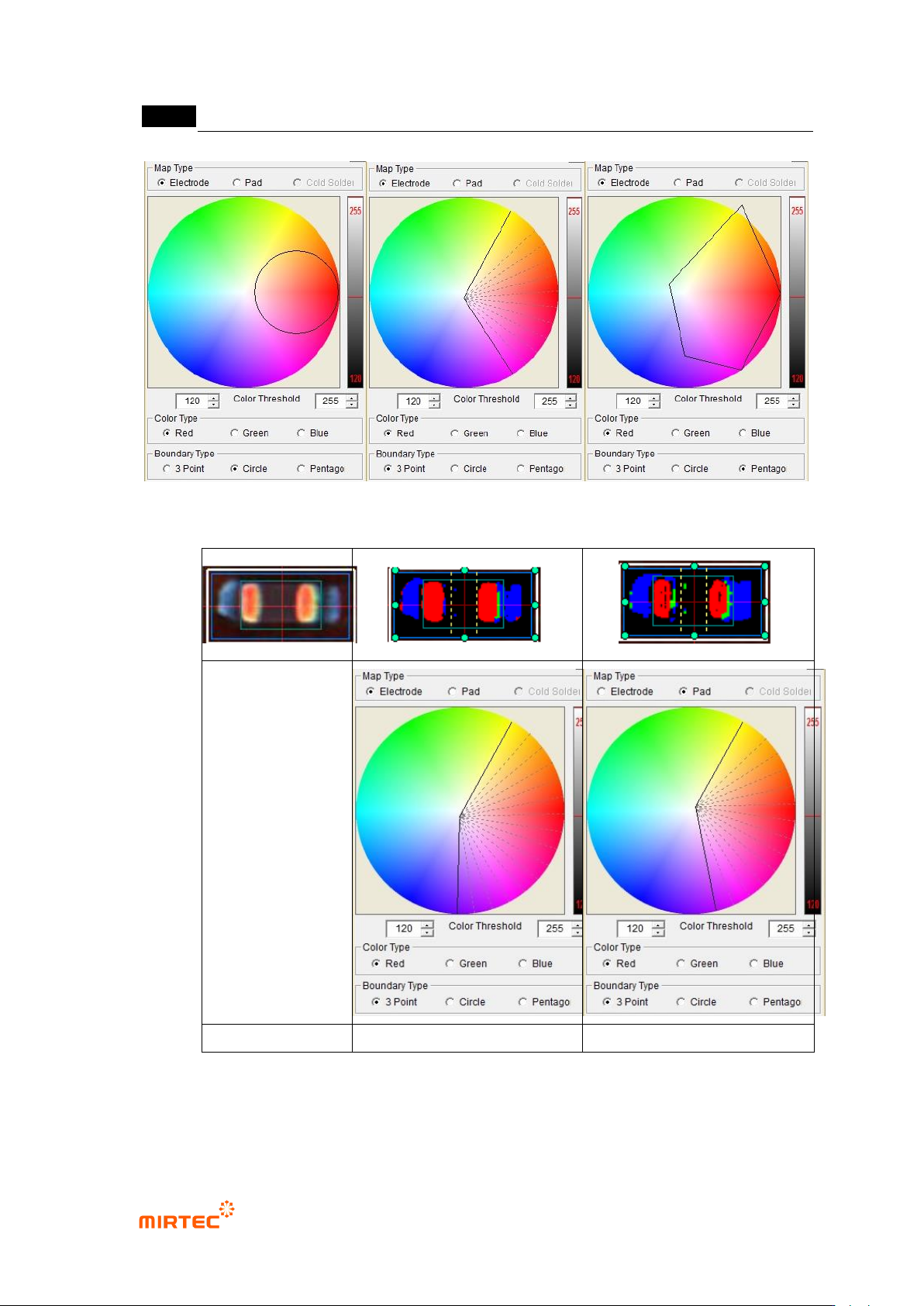
③ Normal boundary region: As shown in [Figure 5-169], type when binarization area is set. 3
points, circle or pentagon can be selected.
[Figure 5-225 color map setting parameter]
MV-9 User Manual
5-184
[Figure 5-226 Example of normal boundary region selection]
chip image
electrode binarization setting
pad binarization setting
[Figure 5-227 Adjustment example of chip electrode and pad color map]
Electrode color ratio