MV-9_Chapter 5. Teaching.pdf - 第188页
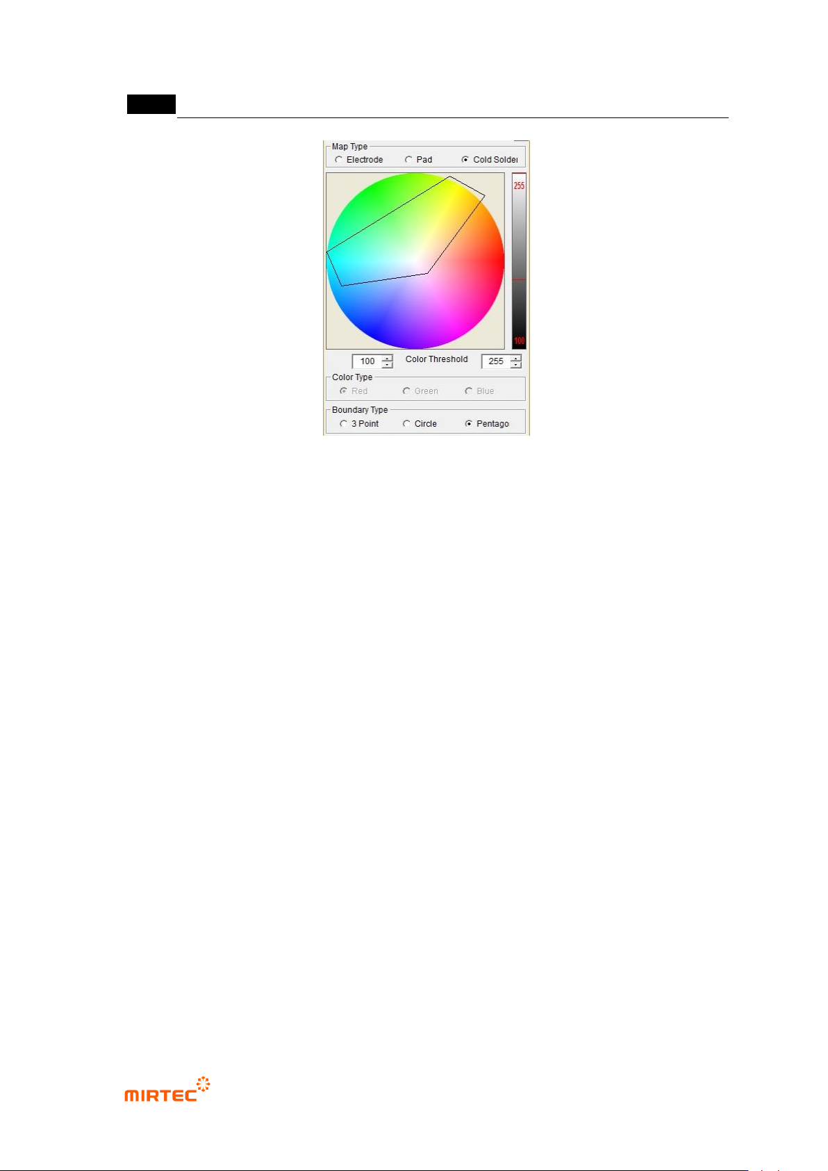
MV -9 Use r Manual 5- 188 [Figure 5- 230 Color map for detection of cold solder _pentag o n setting exampl e] ⑦ Y el low (% ) < - Set cold solder i nspect io n cr i teria param e ter . Y el low ratio in Center Rect. ⑧…
错误!使用“开始”选项卡将 제목 2 应用于要在此处显示的文字。错误!使用“开始”选项卡将 제목 2 应用
于要在此处显示的文字。 .
5-187
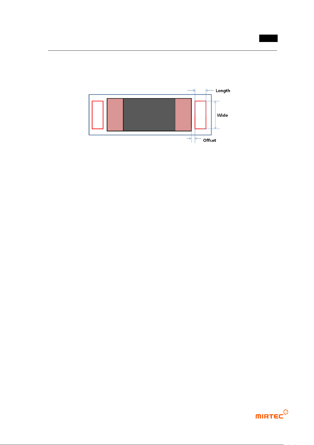
- Length of Center Rect chip length direction.
③ Offset
- This is to set the away distance of Center Rect based on electrode end.
[Figure 5-229 lifted inspection (Center Rect) setting item]
④ Blue Ratio (%): set Blue ratio in Center Rect.
⑤ Red Ratio (%): set Red ratio Center Rect.
⑥ Cold Solder Check
- Set whether to conduct cold solder inspection for chip. In general, for lifted inspection, set
color map to include yellow area (cold solder) in [pad inspection → color map → Pad].
- After setting to detect cold solder defect, If many false defects are occurred during lifted
inspection for Center Rect, separate color map for lifted inspection and cold solder
inspection. The following is separation method.
Exclude yellow area from Pad color map
Select Cold Solder Check in pad inspection tap
Select cold solder in color map, and set only yellow area for cold solder inspection
in color map
- In general, most of cold solder defects displayed in yellow between electrode and pad.
Sometimes, the defect displayed in sky-blue, orange, or pink. Therefore, if necessary,
select pentagon in color map and adjust it as shown in the [Figure 5-247] below.
MV-9 User Manual
5-188
[Figure 5-230 Color map for detection of cold solder _pentagon setting example]
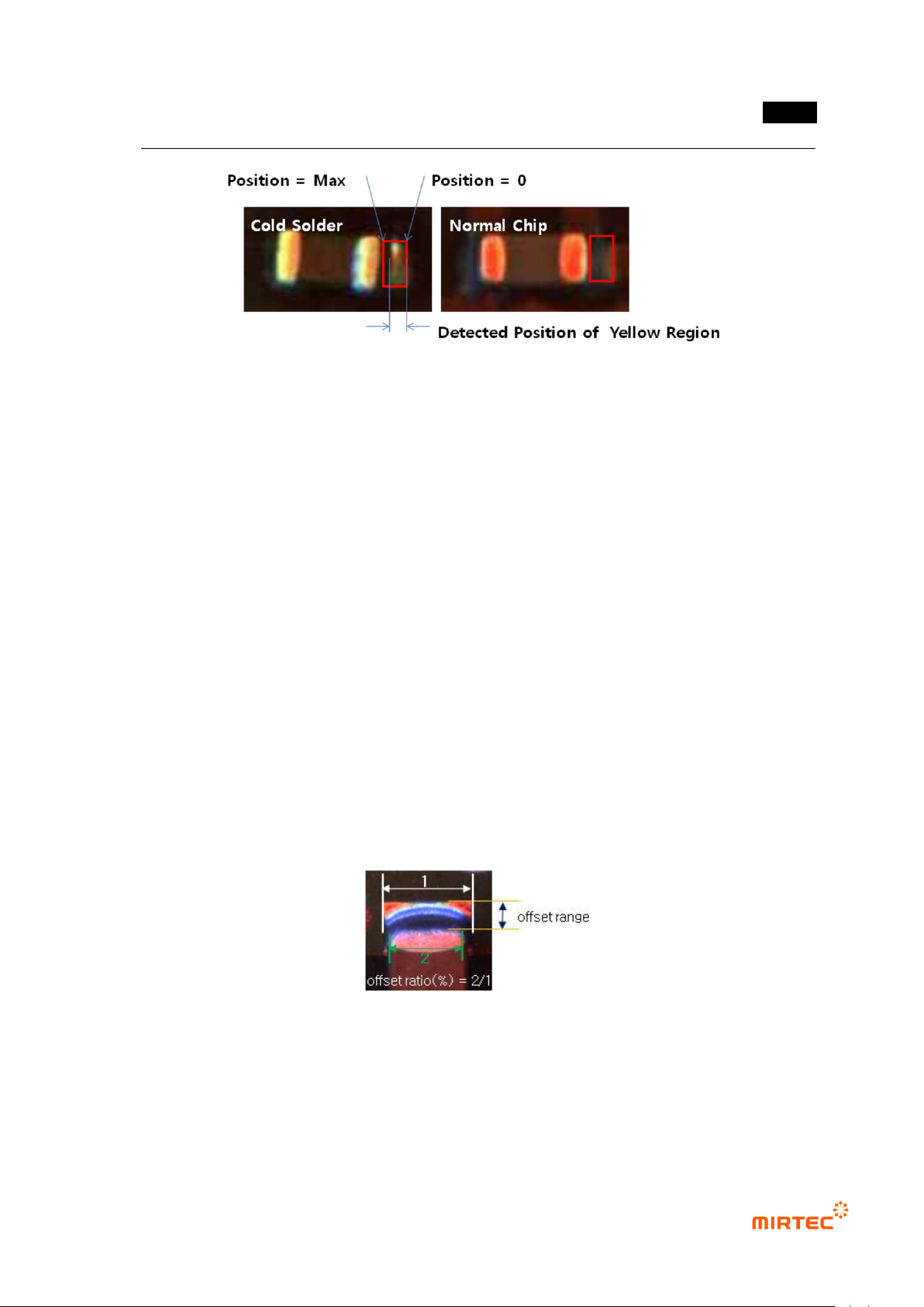
⑦ Yellow (%) <
- Set cold solder inspection criteria parameter. Yellow ratio in Center Rect.
⑧ Position
- Cold solder inspection criteria parameter. Decide the degree of trespass of yellow area to
judge as cold solder in Center Rect. this parameter is used to reduce occurrence of false
defect due to creation of yellow area at outside end of Center Rect.
- If setting value is default value (-1), if it is above setting Yellow (%) regardless of the
position of yellow area, judge as defect. If position value is set to „0‟, that means that
yellow area is located at opposite end of electrode in Center Rect. The larger value is, the
closer yellow area is expanded near electrode. (Refer to [Figure 5-248].).
- For example, If position value is set to „3‟, it is not judged as cold solder even when yellow
area is expanded up to 3 pixels from outside end of Center Rect toward electrode. If
position of yellow detection area is „7‟ under this setting, it means that it is expanded more
closely to electrode than reference position at which yellow area is set and judged as cold
solder defect. Max value of position value is the length of Center Rect.
错误!使用“开始”选项卡将 제목 2 应用于要在此处显示的文字。错误!使用“开始”选项卡将 제목 2 应用
于要在此处显示的文字。 .
5-189
[Figure 5-231 Position parameter for cold solder detection]
⑨ Details
- If red ratio of Center Rect is above reference value, decide whether to judge it as lifted or
not.
- Divided area from electrode end to pad end into 4. If the position of red area extracted
from pad area exits in the first area that is close to electrode, judge as lifted. Besides that,
judge as good.
- When solder is large and thin red due to light effect on a little bit big chip above chip 1005,
this algorithm is displayed in similar shape with lifted by the color map. However, this is set
to use the characteristic that it displayed away from electrode.
Chip shift inspection
- Shift Range is max length for Shift from electrode end to pad end viewing from the length
direction of chip. measure distance from electrode end to pad end during inspection.
- If measurement data is larger than Shift Range setting value, judge as defect. In general,
set Shift Range value as long as pad length.
[Figure 5-232 Offset Ratio definition for Shift inspection]