MV-9_Chapter 5. Teaching.pdf - 第39页
错误 ! 使用“开始” 选项卡将 제목 2 应用于要在此处显示的文字。 错误 ! 使用“开始”选项卡将 제목 2 应用 于要在此处显示的 文字。 . 5- 39 However , foreign m ateri al is darker than pad in vert i cal - horizont al li ght i m age , se lect L for image type, select for binarizat…
MV-9 User Manual
5-38
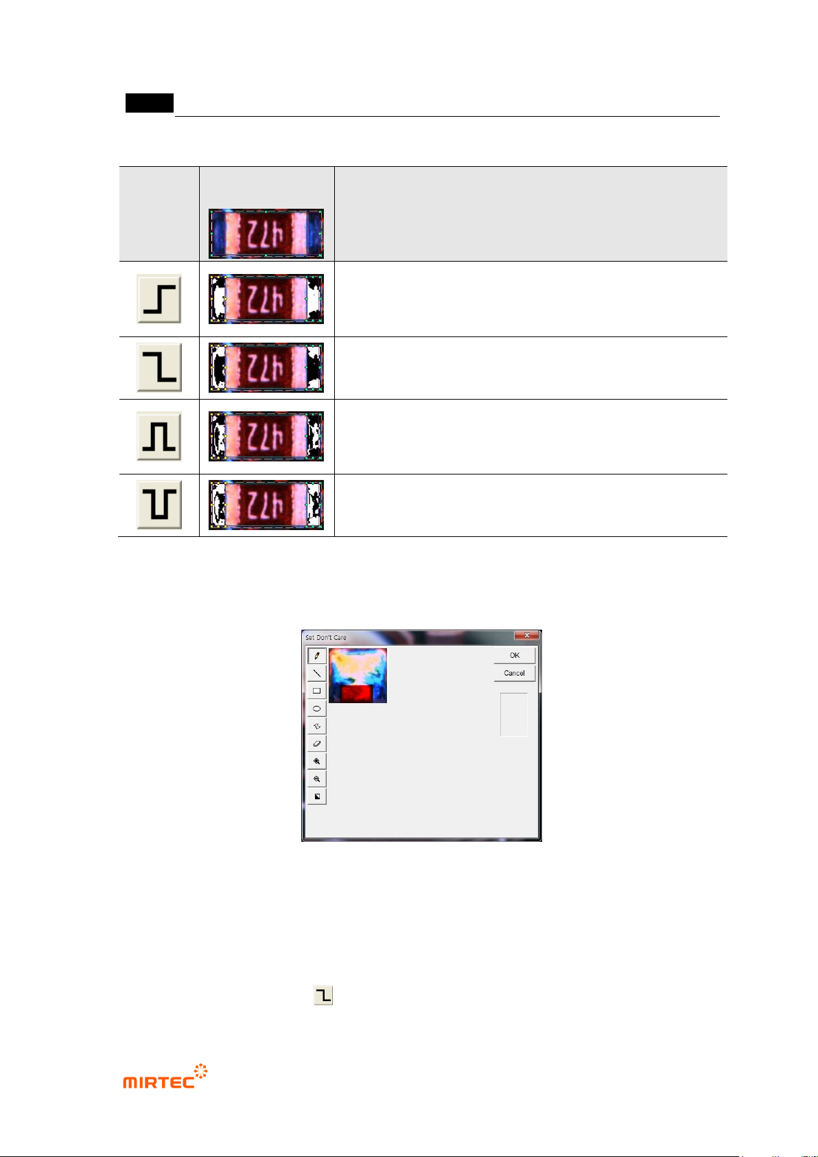
[Table 5-3 4 Binarization methods of solder inspection window]
Status
Binarization
image
Description
Horizontal + vertical light image
binarize all level value below reference to black (0), and all
level value over reference to white (1) based on one
binarization value (Ex: 100)
Binarize all level value below reference to white (1), and all
level value over reference to black (0) based on one
binarization value (Ex: 100).
Binarize all level value within reference range to white (1),
and all level value beyond range to black (0) based on2
binarization value (Ex: 100, 150).
Binarize all level value within reference range to black (0),
and all level value beyond range to white (1) based on2
binarization value (Ex: 100, 150).
‘Don’t care region’
- We can set „Don‟t care region‟ by drawing area in image in inspection window.
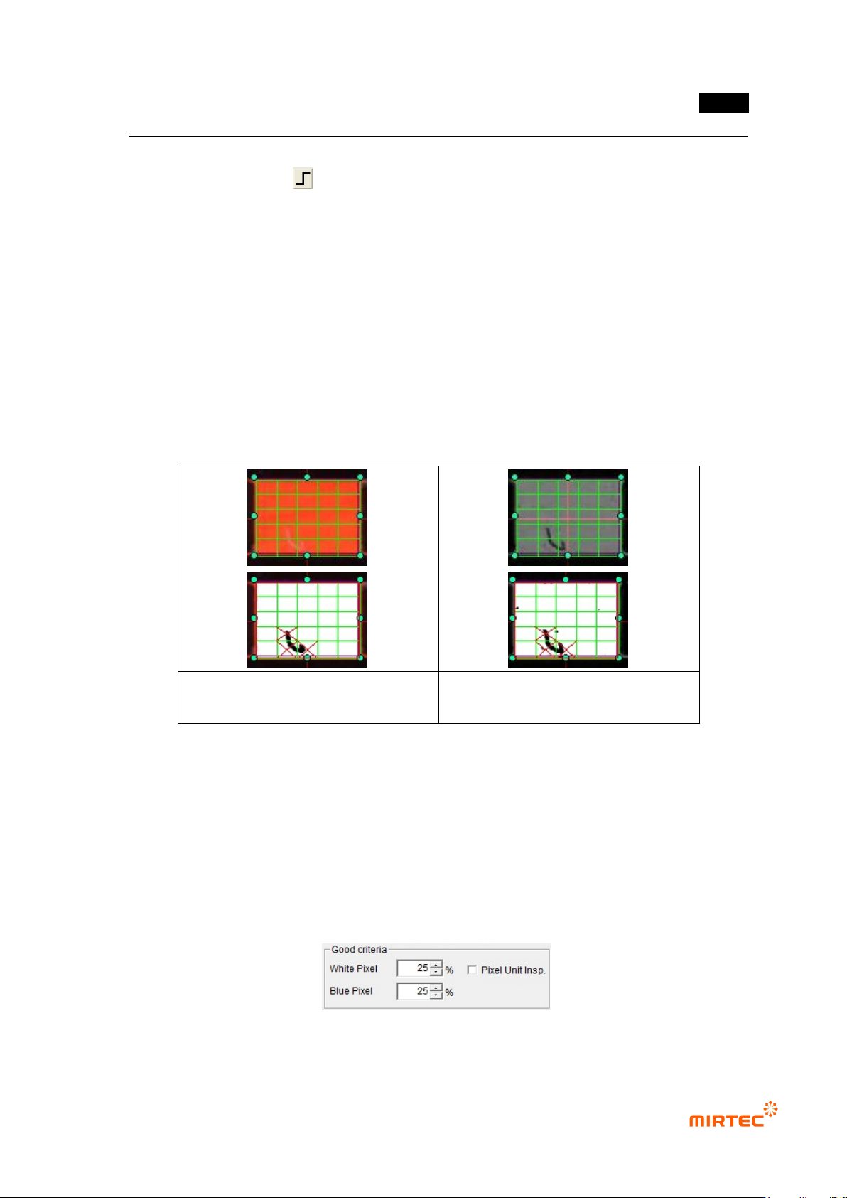
[Figure 5-40 ‘Don’t care region’ setting screen]
Use grid inspection
- Divide solder inspection window with grid and individually inspect each area to detect
solder ball or foreign material on pad.
- Since foreign material on a pad is brighter than pad in horizontal + vertical light, select B or
L for image type, select for binarization method, and adjust binarization value.
错误!使用“开始”选项卡将 제목 2 应用于要在此处显示的文字。错误!使用“开始”选项卡将 제목 2 应用
于要在此处显示的文字。 .
5-39
However, foreign material is darker than pad in vertical - horizontal light image, select L for
image type, select for binarization method and adjust binarization value.
- Enter grid value of width/height in width and height box to divide inside of solder into given
value and to conduct solder inspection for each area.
- Area set as „Don‟t care region‟ will be excluded from inspection.
- [Figure 5-58] shows solder window to which grid function is applied. Inspection will be
performed for each individual segmentation region.
- When grid inspection is used, if each individual grid is smaller than normal reference white
pixel ratio, it will be judged as defect and red X character will be displayed. If the lowest
value among inspection results of each individual grid than normal criteria, inspection
window will be judged as defect.
Defect detection used horizontal +
vertical light
Defect detection used vertical –
horizontal light
[Figure 5-41 Use of grid inspection]
Normal criteria
- White pixel ratio: ratio of reference matching value in white and imaged inspection window.
- Blue pixel ratio: ratio of reference matching value in blue and imaged inspection window.
However, this option can be used only when light type is color.
- Normal criteria must have value higher than reference matching value.
- Pixel unit inspection: unit of normal criteria will be changed to numbers.
[Figure 5-42 Normal criteria setting]
MV-9 User Manual
5-40
Judge good as defect
- This is to set inspection result to normal when it is defect.
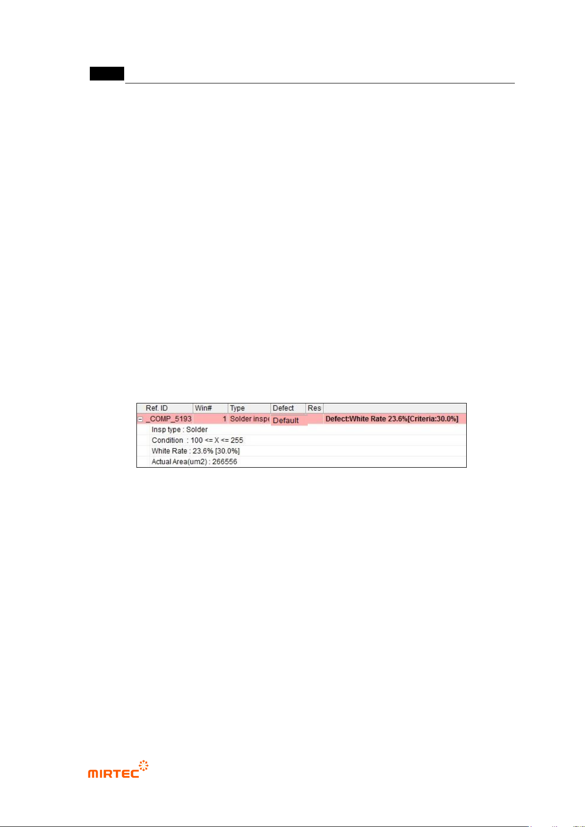
③ Soldering inspection (basic) result in status screen
- To directly inspect solder amount inspection window that completed teaching, select
solder amount inspection window, and select „inspect' item in popup menu displayed by
clicking right button of the mouse. Now, the following inspection result will be displayed
in status screen in the main screen.
Inspection type
- Inspection type
Condition
- White level area during binarization
White pixel ratio
- White area ratio in solder amount inspection window.
- Percent value in brace means ratio value of white area for normal judgment.
[Figure 5-43 Inspection result in status screen]
2) Non-mounting inspection (soldering)
- This is to conduct non-mounting inspection using color information of electrode area and
solder area of chip type component that is soldered.
- In case of normal components, electrode area will be displayed in red. However, if non-
mounting defect occurs, blue ratio increase in electrode area. This characteristic is used to
detect non-mounting defect.
① Teaching method
(a) Draw solder inspection window including solder area and chip electrode, and select
direction.
(b) Select horizontal + vertical light for light type, and basically, „A‟ will be automatically
selected for image type.