MV-9_Chapter 5. Teaching.pdf - 第83页
错误 ! 使用“开始” 选项卡将 제목 2 应用于要在此处显示的文字。 错误 ! 使用“开始”选项卡将 제목 2 应用 于要在此处显示的 文字。 . 5- 83 6) T ap inspection - T ap insp ection is a l gorithm to d etect foreign material on pad and s older ball defect. ① T eaching method (a) Dra…
MV-9 User Manual
5-82
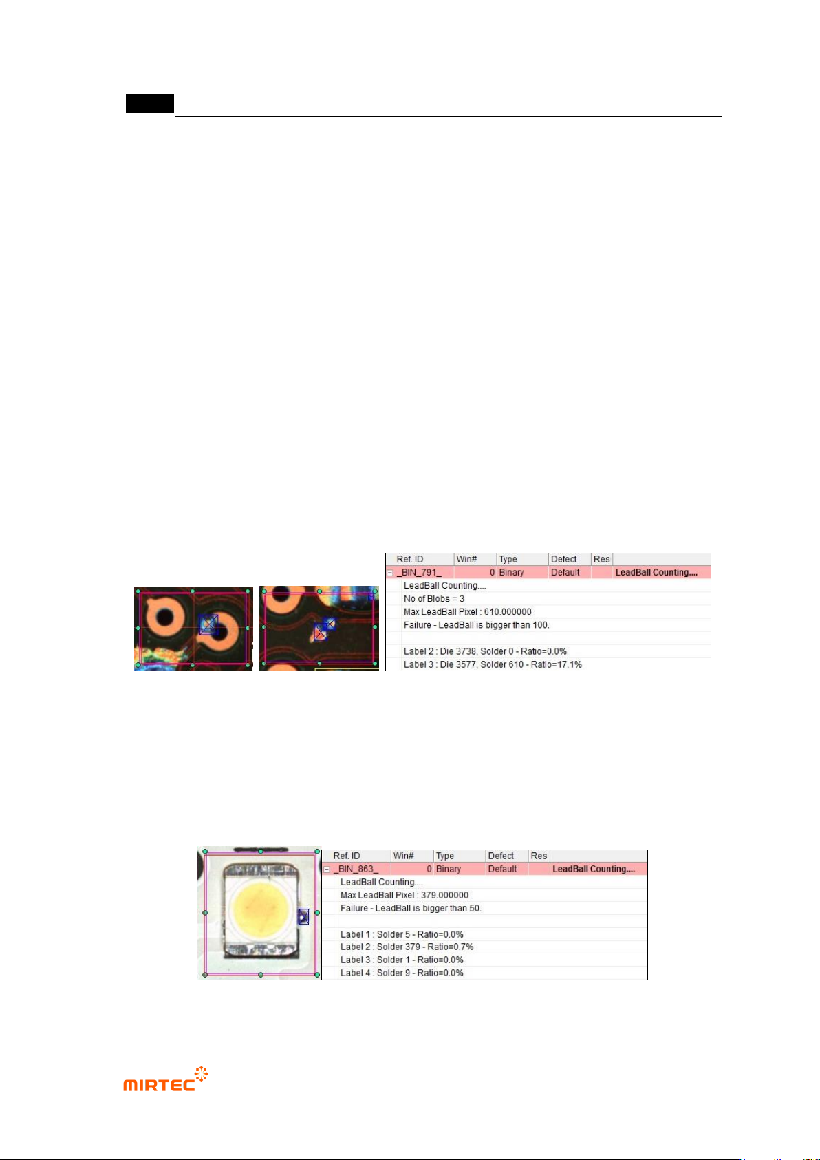
In general, solder ball has small size comparing to total inspection area. Hence,
check at white pixel inspection rather than ratio and enter size value of solder ball
by number of pixel for inspection.
② Inspection result in status screen
Solder ball on pad inspection result
- LeadBall Counting: solder ball inspection algorithm.
- No of Blobs = 3: number of white area displayed in pad Bridge binarization result image.
- Max LeadBall Percentage: ratio of detected solder ball
- Failure – LeadBall is larger than 15: detected solder ball (ratio or number of white pixel) is
larger than reference value 15 and detected as defect.
- Label X: No allotted for No of Blobs = 3. Label 1 is excluded because it is included in „Don‟t
care region‟ setting.
- Die: total area of pad area of Label No X (number of white pixel).
- Solder: area of solder ball detected above Label No X (number of white pixel).
- Ratio: Ratio of solder to die.
[Figure 5-89 Inspection result of solder ball on pad]
Solder ball on substrate inspection result
- Label X: No allotted to solder ball target detected in solder binarization result image.
- Solder: area (number of white pixel) of Label X solder ball.
- Ratio: Ratio of solder to inspection window area.
[Figure 5-90 Solder ball on substrate inspection result]

错误!使用“开始”选项卡将 제목 2 应用于要在此处显示的文字。错误!使用“开始”选项卡将 제목 2 应用
于要在此处显示的文字。 .
5-83
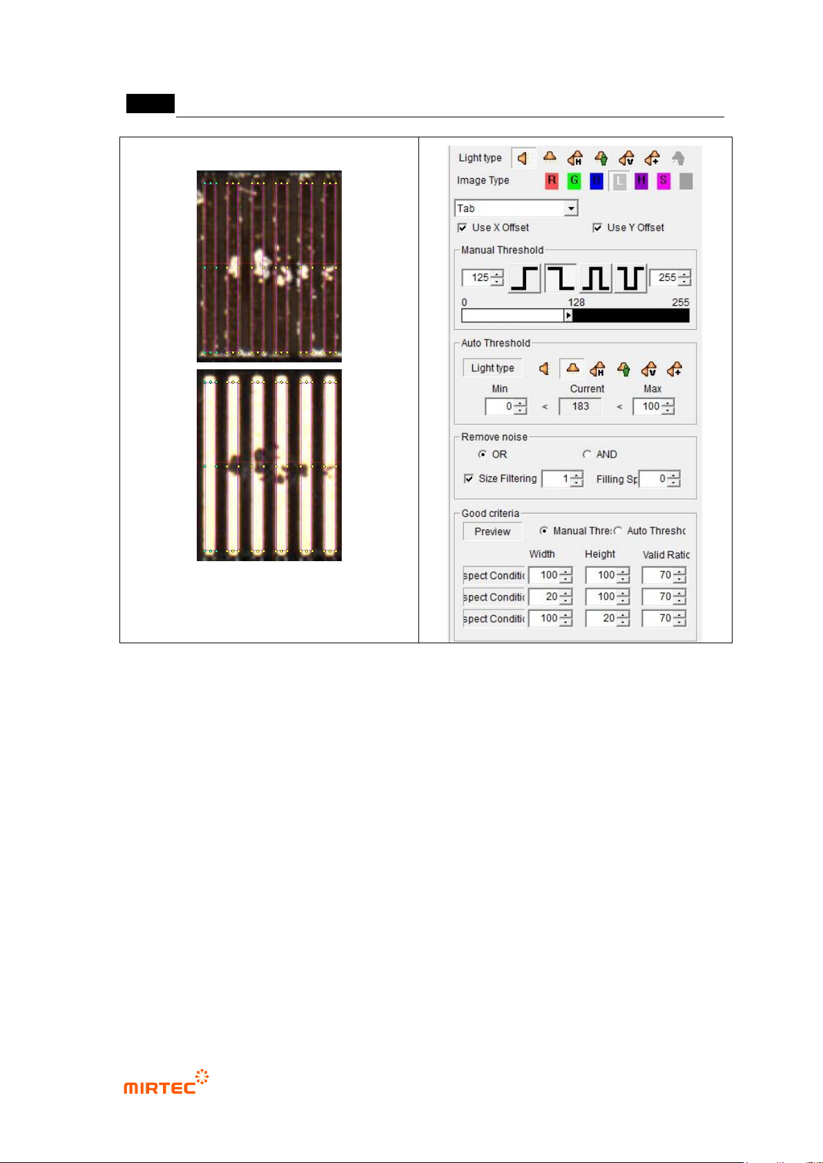
6) Tap inspection
- Tap inspection is algorithm to detect foreign material on pad and solder ball defect.
① Teaching method
(a) Draw binary inspection window in inspection area and select tap inspection for inspection
type.
(b) Select preview in operation window.
(c) Select manual binarization for normal criteria – preview and select default light type and
image type.
(d) Set manual binarization type and binarization value to display tap area in white and to
separate defect over tap to black checking preview image.
(e) Adjust size filtering and space filling for noise removal.
(f) Select auto binarization in normal criteria – preview, and select light for auto binarization.
(g) Conduct trial inspection to display the current value of auto binarization. Adjust min and
max value range based on current value to display defect in black.
(h) Adjust size filtering and space filling for noise removal.
(i) Select binarization or average value or binarization and average value.
(j) Set detection condition for good/defect judgment.
MV-9 User Manual
5-84
manual binarization image auto binarization
image
[Figure 5-91 Teaching example of tap inspection window]
① Parameter description
Tap inspection window
- Do not go over tap area while drawing inspection window.
- For tap inspection, black area is detected as defect in binarization result. Defect over tap
and area that is not tap will be displayed in black by binarization and false defect or whole
of tap teaching region can be judged as defect.
Normal criteria – preview
- Select preview image type displayed in the screen.
- Manual binarization: use image of the selected default light type and image type, and
create preview image by applying manual binarization type and binarization value.
- Auto binarization
Use image of light type selected for auto binarization, and use min-current-max
value set for auto binarization to conduct binarization.