X3_X4_Series machine - 第163页
User manual SIPLAC E X-Series 3 Technical data Software Vers ion SR.601.xx 11/ 2005 US Ed ition 3.12 PCB single conveyor 163 3.12 PCB single conv eyor The placeme nt mach ine is sup plied with a single PCB conveyo r as s…

3 Technical data User manual SIPLACE X-Series
3.11 Vision cameras Software Version SR.601.xx 11/2005 US Edition
162
3.11.5.3 Fiducial criteria
3
3
3.11.5.4 Ink spot criteria
3
Locate 2 fiducials
Locate 3 fiducials
X-/Y-position, rotation angle, mean PCB distortion
in addition: shear, distortion in X- and Y-direction separately
Fiducial shapes Synthetic fiducials: circle, cross, square, rectangle, rhombus,
circular, square, and rectangular contours, double cross
any pattern
Fiducial surface
Copper
Tin
Without oxidation and solder resist
Warp ≤ 1/10 of structure width, both with good contrast to
environment
Dimensions of synthetic fiducials
Min. X/Y size for circle and rectangle:
Min. X/Y size for annulus and rectangle:
Min. X/Y size for cross:
Min. X/Y size for double-cross:
Min. X/Y size for rhombus:
Min. frame width for annulus and rectangle:
Min. bar width / bar distance for cross, double-cross:
Max. X/Y size for all fiducial shapes:
Max. bar width for cross, double-cross:
Min. tolerances, general:
Max. tolerances, general:
0.25 mm
0.3 mm
0.3 mm
0.5 mm
0.35 mm
0.1 mm
0.1 mm
3 mm
1.5 mm
2% of nominal dimension
20% of nominal dimension
Dimensions of patterns
Min. size
Max. size
0.5 mm
3 mm
Fiducial environment Clearance around reference fiducial not necessary if there is no
similar fiducial structure in the search area.
Methods - Synthetic fiducial recognition method
- Mean grayscale value
- Histogram method
- Template matching
Shapes and sizes of fiducials/
structures for
synthetic fiducials
other methods
For dimensions of synthetic fiducials,
see Section 3.11.5.3
Fiducial criteria
min. 0.3 mm
max. 5 mm
Masking material Good coverage
Recognition time Depends on the method: 20 ms - 0.2s
User manual SIPLACE X-Series 3 Technical data
Software Version SR.601.xx 11/2005 US Edition 3.12 PCB single conveyor
163
3.12 PCB single conveyor
The placement machine is supplied with a single PCB conveyor as standard. The dual PCB con-
veyor is available as an option from the factory (see Section 3.13
, page 166). The left or the right
side of the PCB conveyor can be used as the stationary side, as required.
The conveyor belts are driven by DC motors. There is a lifting table for clamping the PCBs in each
processing area. The PCB conveyor width can either be set from the user interface or preset in
the placement program.
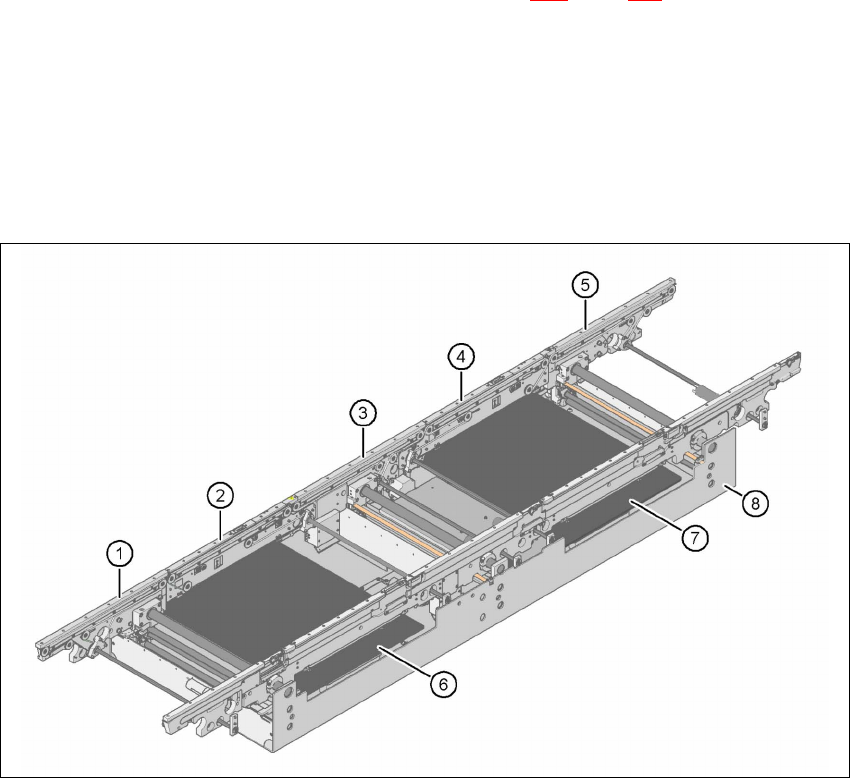
3.12.1 Structure
3
Fig. 3.12 - 1 Structure of the PCB single conveyor
(1) Input conveyor
(2) Processing conveyor 1
(3) Intermediate conveyor
(4) Processing conveyor 2
(5) Output conveyor
(6) Lifting table 1
(7) Lifting table 2
(8) Assembly trough

3 Technical data User manual SIPLACE X-Series
3.12 PCB single conveyor Software Version SR.601.xx 11/2005 US Edition
164
3.12.2 Technical data
3
3
3.12.3 Description of the functions
For placement, the PCB is clamped from below. The distance between the top of the PCB and the
placement head thus remains unchanged for each PCB, and is not dependent on the thickness of
the PCB. The placement rate is thus independent of the PCB thickness. The PCB fiducial center-
ing can also be optimized. Since the distance between the PCB surface and the PCB camera re-
mains the same, the PCB camera is always focussed on the PCB surface with the same
sharpness. The PCB fiducial contours are optimally mapped on the CCD chip of the PCB camera.
The width of the circuit board conveyor is set and monitored by an integral control circuit. It can
be selected by calling up the program. The control circuit then actuates the stepping motors until
the desired width is reached. The width adjustment is therefore independent of other machine
components.
Fixed conveyor side Right or left
PCB format
Standard (LxW)
Wide board configuration
Long board option
50 x 50 mm² to 450 x 450 mm² (item no. 00119625-xx)
50 x 50 mm² to 450 x 508 mm² (item no. 00119629-xx)
50 x 80 mm² to 610 x 508 mm² (item no. 00119672-xx)
PCB thickness
Standard 0.3 mm to 4.5 mm ± 0.2 mm
(thicker PCBs available on request)
Max. PCB warpage Up: 6 mm - PCB thickness
Down: 0.3 mm + PCB thickness
PCB weight Max. 3 kg
Clearance on PCB underside
Standard
Option
25 mm ± 0.2 mm
Max. 40 mm ± 0.2 mm
Component-free PCB handling edge 3 mm
PCB changeover time < 2.5 s
PCB positioning accuracy ± 0.5 mm
PCB transport height 830mm ± 15mm (standard)
900mm ± 15mm (optional)
930mm ± 15mm (optional)
950mm ± 15mm (SMEMA: optional)
Type of interface SMEMA / SIEMENS
Bad fiducial detection Possible
Automatic width adjustment Possible