OM-1650-001_w - 第18页
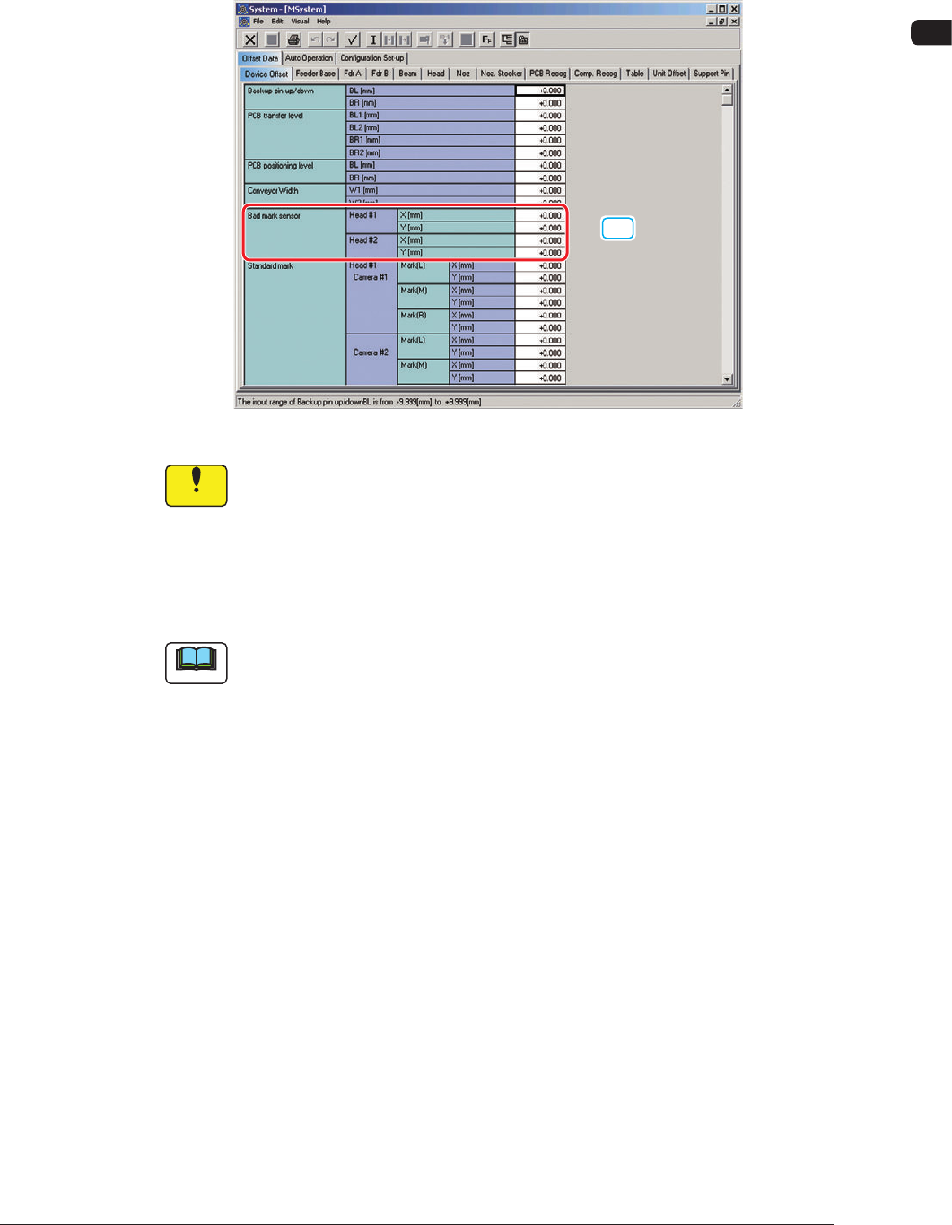
OM-1650 15 7. Offset Data 7. Of fset Data The "Bad Mark Sensor" column is added in the "Device Offset" tab sheet in "Offset Data". [1] "Device Offset" Tab Sheet F11 Notice They hav…
OM-1650
14
6. Pattern Program
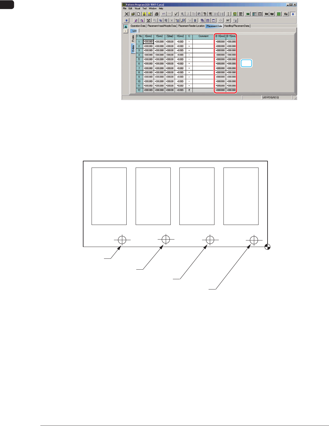
6.3 Placement Data (O Data)
When "Mode" in "Unit PCB BBR" is set to "Optional", set "B-X" and "B-Y" in
the Placement Data (O Data).
[1]
"Placement Data (O Data)" Tab Sheet F9
[1] B-X[mm] and B-Y[mm]
Set the coordinates of each bad mark based on the placement coordinates
reference.
Placement Coordinate
Reference
Bad Mark of Pattern 1
Bad Mark of Pattern 2
Bad Mark of Pattern 3
Bad Mark of Pattern 4
Pattern 4
(B-X
4, B-Y4)
Pattern 3
(B-X
3, B-Y3)
Pattern 2
(B-X
2, B-Y2)
Pattern 1
(B-X
1, B-Y1)
F10
1006-001
OM-1650
15
7. Offset Data
7. Offset Data
The "Bad Mark Sensor" column is added in the "Device Offset" tab sheet in
"Offset Data".
[1]
"Device Offset" Tab Sheet F11
Notice
They have been adjusted and set before the machine is delivered, so do
not unnecessarily change them.
[1] Bad Mark Sensor
The deviation between the designed position and actual position of the bad
mark sensor installation is adjusted.
Note
When SIGMA-G4 is used, the Head 1 are not displayed on the screen.
1006-001
OM-1650
16
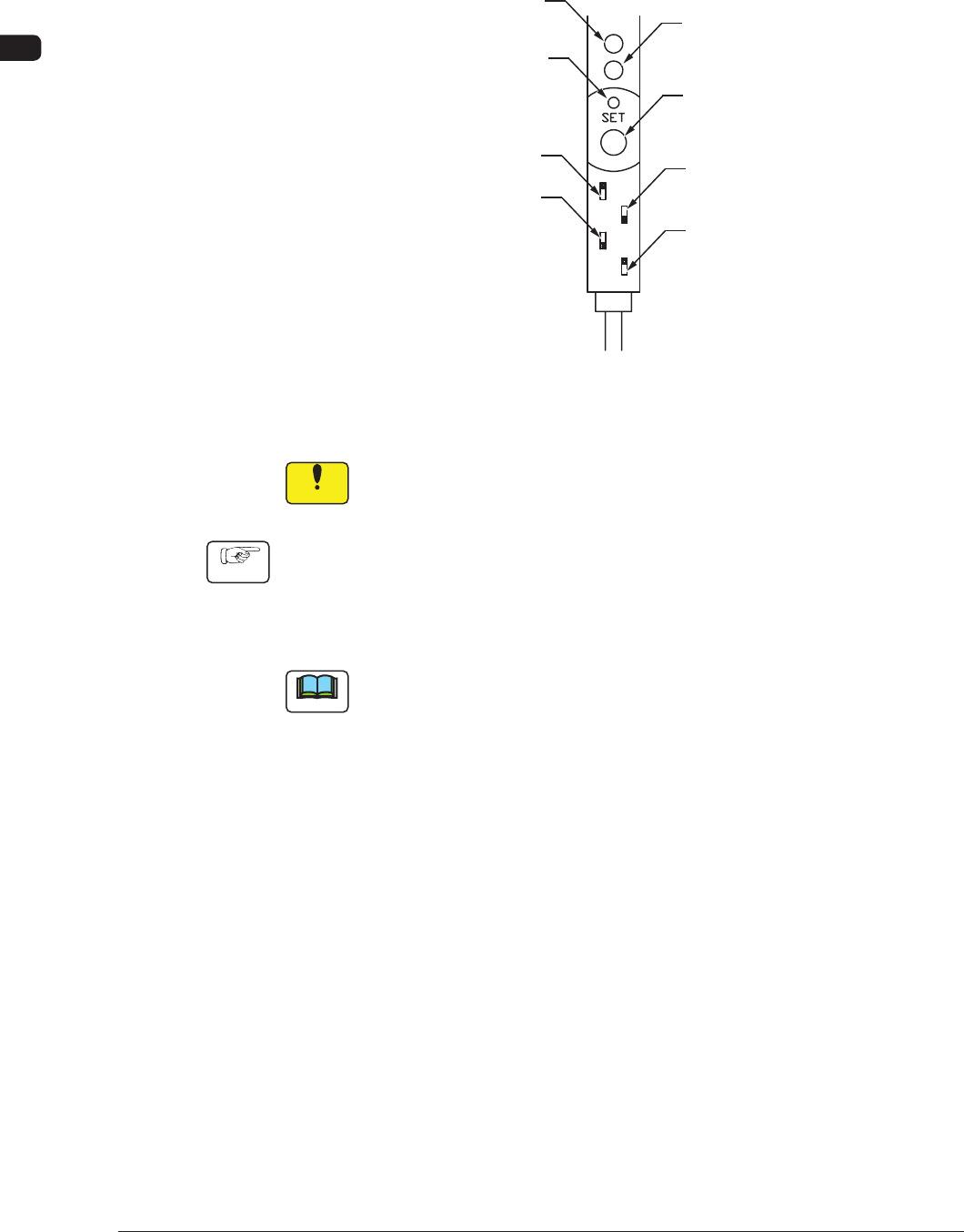
8. Procedure for Bad Mark Sensor Adjustment
8. Procedure for Bad Mark Sensor Adjustment
When the sensor system is used in the bad mark detection function, the adjustment
of the bad mark detection sensor is to be performed.
Mode Indicator
(Red LED)
Tuning Indicator
(Yellow LED)
Key-Protect Switch
Stability Indicator
(Green LED)
[SET] Button
Output Selector Switch
FINE/TURBO SW
Output Timer SW
Amplifier of Bad Mark Sensor F12
Procedure for Bad Mark Sensor Adjustment
Notice
Do not change the dip switch settings.
Procedure
(1) Change to the current pattern program (the program for current production)
and perform the setup operation.
(2) Put a bad mark on the PCB to be produced.
Note
(a) Use a black mark as a bad mark for a comparatively bright PCB detection
area (PCB with a lot of light reflex).
Use a white mark as a bad mark for a comparatively dark PCB detection
area (PCB with a little light reflex).
(b) When the selection is changed (from "Black Mark" to "White Mark" or
vice versa), be sure to change the mark image ("Black (E/NR)" or "White
(E/R)" in the related "Mark Image" text box of the pattern program data.
(3) Transfer the PCB to be produced to the PCB positioning section.
1006-001