OM-1650-001_w - 第30页
OM-1650 27 1 1. Bad Mark Communication Function 1 1.1 "Product." Window [1] [3] [2] F25 [1] PCB ID Display When the communication in the input machine has been set to "Enable", the "PCB ID" …
OM-1650
26
11. Bad Mark Communication Function
11. Bad Mark Communication Function
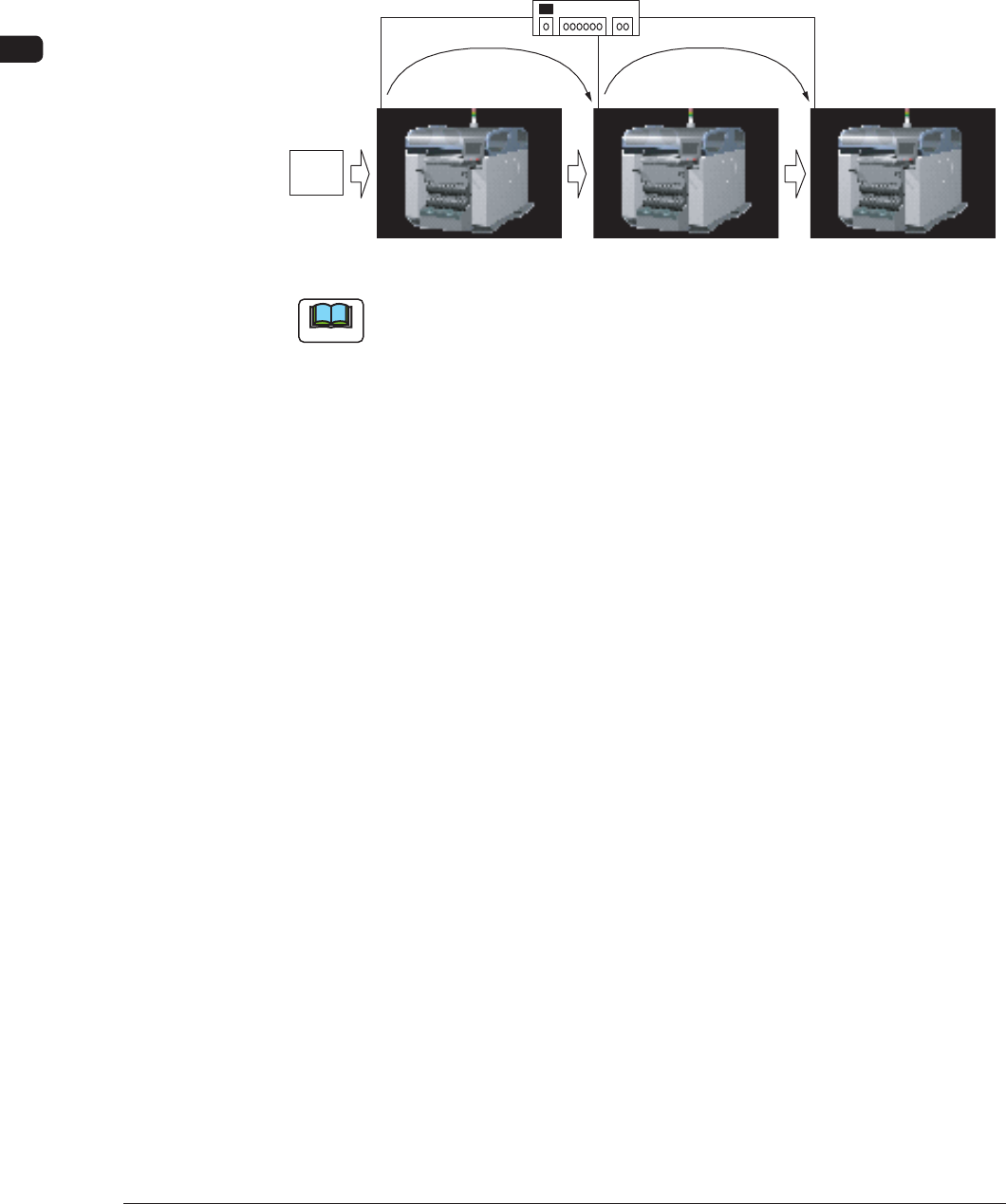
This function detects a bad mark in the optional device and transmits the detection
results to the output machine to use.
The shorten cycle time is realized by means of eliminating the bad mark detection
using the sensor/camera in each device before the production.
Bad Mark Information
PCB
Bad Mark Information
Switching Hub
Ethernet LAN
F24
Note
When this function is to be used, it is prerequisite that the "Line Config" Tab
Sheet has been setup in advance in the "MACH SETUP" Window for the device.
1006-001
OM-1650
27
11. Bad Mark Communication Function
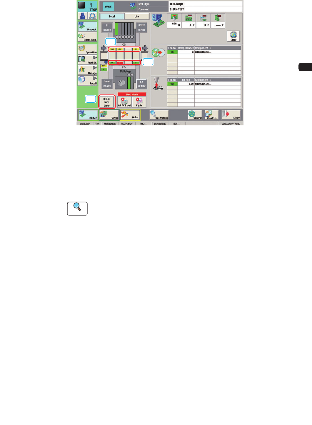
11.1 "Product." Window
[1]
[3]
[2]
F25
[1] PCB ID Display
When the communication in the input machine has been set to "Enable", the
"PCB ID" received from the input machine is displayed.
When the communication in the input machine has been set to "Disable", the
"PCB ID" created in the machine is displayed.
Reference
Refer to "11.2 OPERATION Window" for the input machine
communication setup.
[2] Defective PCB Count Display
The No. of defective PCBs in the PCBs to be produced is displayed. When
there is no defective PCB, the background color is turned green and when
there is any defective PCB, the background color is turned red.
1006-001
OM-1650
28
11. Bad Mark Communication Function
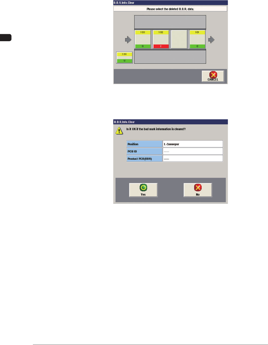
[3] [BBR Info Clear] Button
When this button is pressed, the unit selection window for the "BBR Info
Clear" is displayed. There, the unit where the bad mark data is to be deleted,
can be selected.
F26
When the unit where the bad mark data is deleted, is selected, the "BBR Info
Clear" execution window appears, where the bad mark data can be deleted.
F27
1006-001