OM-1650-001_w - 第8页
OM-1650 5 3. Rough View of Machine 3. Rough V iew of Machine PEC Recognition Camera Bad Mark Sensor Amplifier F1 Note The bad mark detection sensor for SIGMA-G4 is to be attached to the head No. 2 and the bad mark detect…

OM-1650
4
1. Scope
1006-001
1. Scope
When a bad mark is placed on any unit PCB in a multi-unit PCB with the same
repetitive patterns for each unit PCB, then, this function prevents the component
placement on such unit PCB.
The bad mark detection function includes Bad Mark Detection on Each Unit PCB,
as well as Master Bad Mark detection.
A bad mark detection photo-sensor or PEC recognition camera is used to detect a
bad mark.
2. Functions
•
Bad Mark Detection on Each Unit PCB
The bad mark detection photo-sensor or PEC recognition camera detects a bad
mark on a unit PCB and the machine automatically determines whether or not
the components should be placed on that unit PCB according to the results of
the detection.
A bad mark can be located on any position within the specified area on a unit
PCB.
•
Master Bad Mark Detection
The bad mark detection photo-sensor or PEC recognition camera detects
whether or not there is a bad mark on the multi-unit PCB in question. Then,
according to the results of the detection, the bad mark on any unit PCB is
detected and the machine determines whether or not the components should be
placed on that unit PCB.
This function shortens the time required for the BBR detection.
OM-1650
5
3. Rough View of Machine
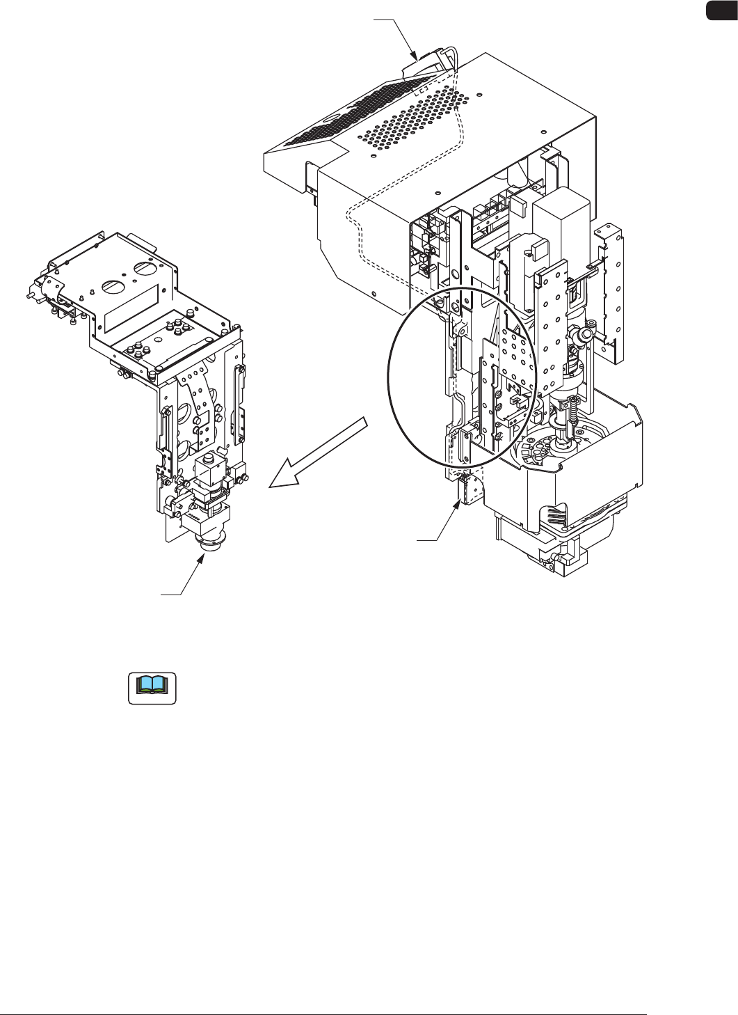
3. Rough View of Machine
PEC Recognition
Camera
Bad Mark Sensor
Amplifier
F1
Note
The bad mark detection sensor for SIGMA-G4 is to be attached to the head No.
2 and the bad mark detection sensor for SIGMA-G5 is to be attached to the Head
No. 1 or Head No. 2.
1006-001
OM-1650
6
4. Scope of Actions
4. Scope of Actions
(1) When the automatic operation is started, the placement head is moved so that
the bad mark detection sensor or PEC recognition camera is aligned with the
bad mark position set in the pattern program.
(2) After the movement, the bad mark detection sensor or PEC recognition
camera detects whether or not there is any bad mark on the multi-unit PCB.
(3) Whether or not there are bad marks on any of the repetitive patterns is
detected according to the pattern program data.
(4) When all bad marks have been detected, the machine starts the component
placement operation. At this stage, the machine does not place any
component on any unit PCB where a bad mark has been detected in the
above steps (1) through (3).
Note
(a) When the "Mode" in the "Overall BBR Detection" has been set to "Enable"
in the pattern program, at first, the master bad mark detection is performed.
In the case that a master bad mark is not detected, the PCB is determined
as a good PCB. In this case, the machine starts the component placement
operation without performing the bad mark detection on any unit PCB.
(b) In the case that the function detects a bad mark on all unit PCBs of a multi-
unit PCB placed on the positioning section, then the machine will not place
any component on any unit PCB. It will stop in an error condition.
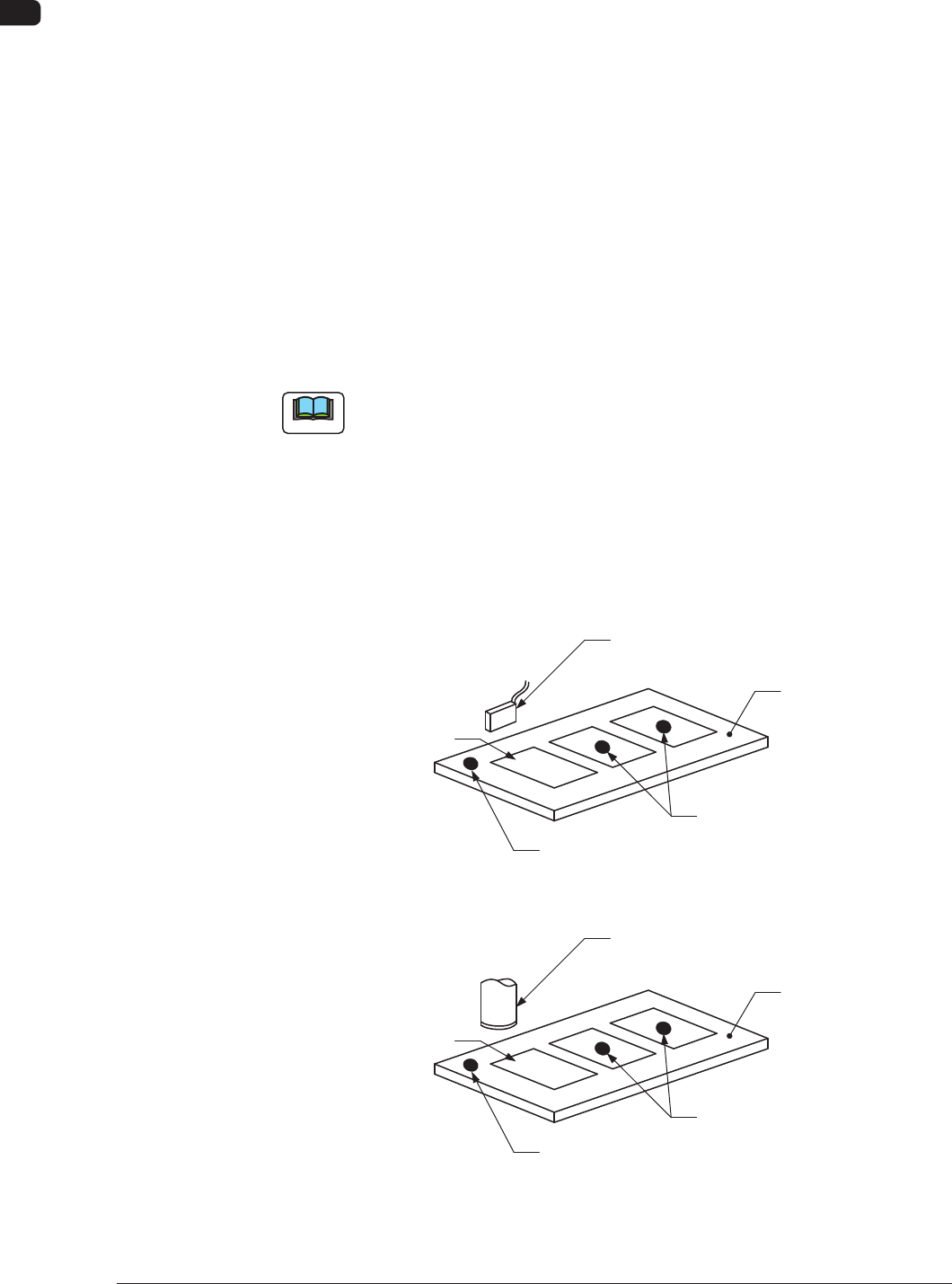
Unit PCB
Bad Mark Sensor
Bad Marks
PCB
Master Bad Mark
In Sensor Mode F2
Master Bad Mark
Unit PCB
PEC Recognition Camera
Bad Marks
PCB
In Camera Mode F3
1006-001