OM-1646-001_w.pdf - 第81页
62 OM-1646 1005-001 17.Specications 17. Specications Item Description 1. Model Name GS-CU200 2. Applicable Model SIGMA-G5 3. PCB Flow Direction and T ransfer Reference PCB Flow Direction : From Left to Right / From R…
61
OM-1646
1005-001- (1094802002-2)
X5504
X5508
AE-LINK
Converter
U181(L)
A55
CN8
CN4
CN1
X5501
CN5
X5505
X5510
CN10
N2 N1
X5509
CN9
X12763
UB77:X2763
1091401300-09
2091401304-02
X16204
A162
CN4
M162
CN1
X16201
M
NA-W2
X16210
CN10
N2 N1
X16209
CN9
X5104
X5108
A51
CN8
CN4
CN1
X5101
M
NR-LB1
M52
CN5
X5105
M
NR-LB2
X5110
CN10
N2 N1
X5109
CN9
X4904
X4908
B5101
B5101
A49
CN8
CN4
M49
CN1
X4901
M
NR-LA1
M50
CN5
X4905
M
NR-LA2
X4910
CN10
N2 N1
X4909
CN9
X4304
X4308
A43
CN8
CN4
M43
CN1
X4301
M
NA-LA1
M44
CN5
X4305
M
NA-LA2
1091401300-08
BA Side Panel TB:DC1
X14906
X4310
CN10
N2 N1
X4309
CN9
X1402
X1300F1
2091401304-02
M55
M
NA-BBL
M56
M
NA-BBR
CN3
X5503
CN7
X5507
B5501
B5601
B16203
B16201
B4401
B4301
B4401
B4301
X0840
X0841
B4901
B4901
M51
CN2A/2BCN1A/1B
/RX
RX
/TX
TX
9,10
7,8
5,6
3,4
/RX
RX
/TX
TX
9,10
7,8
5,6
3,4
U14
X1440
CN40
X1441
CN41
X1433
CN33
X1437
X1436
CN36
CN37
X1439
CN39
Y1436
Y1437
Y1439
X0803
CN4
CN3
BA Side Panel TB:DC1
1091401300-08
X0801 X0802
B4301
B4401
X1412
CN12
B1412,1413
X1413
CN13
B1412
B1413
HLS Collective Section(U12):X1202
X1300F1
1091401300-11
2091401304-02
R
X1410
CN10
B1410,1411
X1411
CN11
B1410
B1411
X1432
CN32
X1435
X1434
CN34
CN35
X1438
CN38
Y1434
Y1435
Y1439
X0816
CN16
B1416,1417
X0817
CN17
B1416
B1417
X1414
CN14
B1414,1415
X1415
CN15
B1414
B1415
1091401300-08
BA Side Panel TB:DC1
X14906
PCB Stopper Origin: AL
PCB Stopper Upper: AL
PCB Stopper Origin: AR
PCB Stopper Upper: AR
Lane A Stop Sensor A Mounting Section 1
Lane A Stop Sensor A Mounting Section 2
Lane A Stop Sensor
Lane B Stop Sensor
Movable Chute 2 Origin Sensor
Backup 3 Origin
Backup 4 Origin
Bank Feeder Change Cart
Connector Section (F)
PCB Stopper Origin: BL
PCB Stopper Upper: BL
PCB Stopper Origin: BR
PCB Stopper Upper: BR
Transfer L (UB32)
Bank Feeder Change Cart
Connector Section (F)
Movable 3 Z Clamp
Down: L
Movable 3 Z Clamp Up: L
PCB Stopper Lane A: R
Movable 1.2 Z Clamp
Down: R
Movable 1.2 Z Clamp Up: R
PCB Stopper Lane B: L
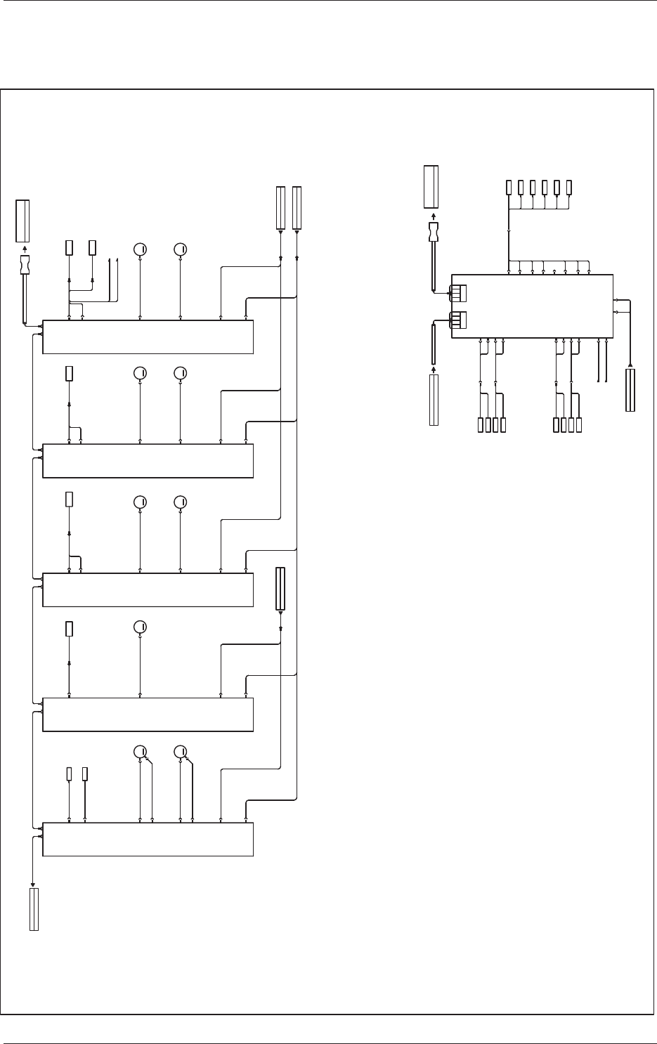
16.5 Cable Connection Diagram
Dual Transfer Harness Connection Diagram 2
62
OM-1646
1005-001
17.Specications
17.Specications
Item Description
1. Model Name GS-CU200
2. Applicable Model SIGMA-G5
3. PCB Flow
Direction
and Transfer
Reference
PCB Flow Direction : From Left to Right / From Right to Left
(Selected when shipped from the factory)
Transfer Reference : Front Left / Front Right
(Selected when shipped from the factory)
4. Applicable PCB
Mode Dual Transfer Mode Single Transfer Mode
Dimensions
X × Y
50 × 50 to 610 × 216 mm 50 × 50 to 610 ×
381 mm
Note : Four Corners : R1 to R1.5 mm
T
ickness
0.3 to 5.0 mm
Mass
Max. 1.5 kg (50 <= X <= 260 mm)
Max. 2.5 kg (260 < X <= 610 mm)
Material
Glass Epoxy
Ceramic (Option)
Notes : (a) In the case of ceramic, separate examination is required.
(b) D
epending on the PCB material, shape, warpage, mass or
surface condition (gloss), etc., it should be tested whether
or not the PCB can be transferred, or the components can
be placed normally, to conrm.
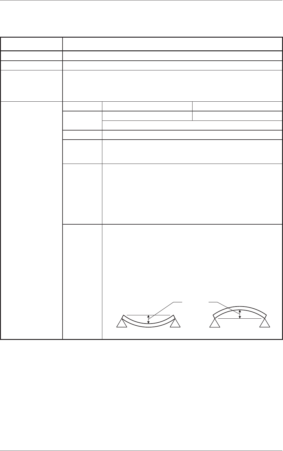
Warpage
0.2 mm or less per 50 mm (unit length)
Upper : Max. 1.0 mm
Lower : Max. 1.0 mm
• 0.2 mm or less per 50 mm (unit length)
Example: The warpage must be 0.8 mm or less when the PCB
size is 200 mm.
• Max. 1.0 mm
Example: The warpage must be 1.0 mm or less when the PCB
size exceeds 250 mm.
Warpage
63
OM-1646
1005-001
17.Specications
Item Description
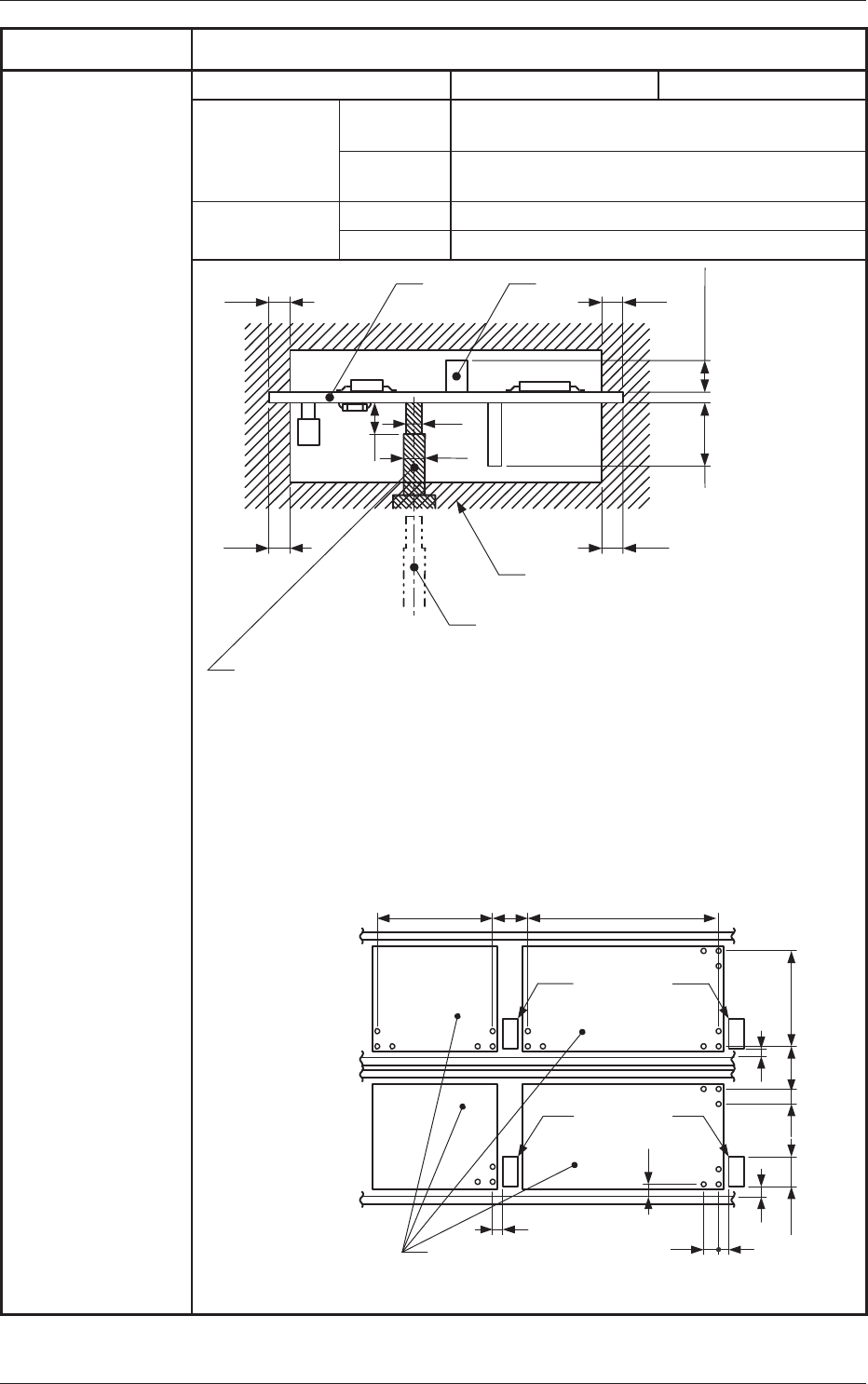
5. Conditions of PCB
before Placement
(Regulation
of Component
Height)
Dual Transfer Mode Single Transfer Mode
Height of
Previously-
Placed
Component
Upper Surface
12.7 mm / High-Speed Head
25.4 mm / Multifunctions Head
Lower Surface
30 mm
Dead Space
Upper Surface
3.0 mm
Lower Surface
3.0 mm
3.0
PCB
PCB Support Pin (At this position when
PCB is transfered.)
Previously-placed Components
Unallowed Range
Component
3.0
PCB Support Pin (Several Places)
φ5
φ2
4.0
3.0 3.0
When the
High-Speed
Head is used:
Max. 12.7
When the Multi-
Functional Head
is used:
Max. 25.4
Max. 30
(Front Side of Machine)
Unit : mm
Notes : (a) The gure shows that the PCB is being supported.
(b) Set the PCB support pin on the position where it does not touch the
already placed component.
(c) The dimensions are those for design reference.
Leave some room for the actual setting.
(d) PCB support pin position can be moved "10mm" by "10mm".
(e) For the positional relationship between the conveyor, PCB stopper and
backup base, refer to the following gure.
200
51
50
250 300
9
1030.5
5
10
Movable A
PCB
Positioning
Stopper
Backup Base
510
9
(Dual Transfer Mode, Flow Direction from left to right)
Movable A'
Movable B
Movable B'
PCB
Positioning
Stopper
Unit : mm