SM-131-006.pdf - 第159页
Device Name Chip Mounter Block Name Page No. Unit Name Revision Model Item GXH-1 Chapter 6 Backup Base Section 0406-001 6-8
Device
Name
Chip Mounter
Block Name
Page No.
Unit Name
Revision
Model ItemGXH-1
4. Backup Base Offsets
Chapter 6 Backup Base Section
4.1 Backup Base Offsets
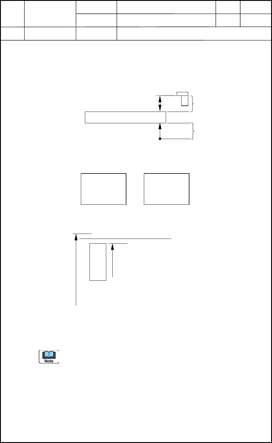
• Clearance after Upward Movement (48.5 mm) of Base from Origin Position: 44 mm
(Design Value)
• Measuring Spots: Position of "Conveyor Width = 300 mm", 4 places for each base
Offset Values Entered (Example)
Minus
Upper Surface of PCB
Plus
Actually Measured Value 43.95 ----- Offset +0.05
Actually Measured Value 44.05 ----- Offset -0.05
Manual Alignment Operation
(1) Follow the operation sequence ([MAINT] Button → [DVC CHECK] Button →
[MOTOR] Button → [Block5] (Others) Button → [NA-LL1] or [NC-LR1] Button).
Movement by Relative Value: Travel 44 mm
Confirm that there is no support pin on the backup base.
(2) Select the [-] button and press the [start] button.
Entry Destination (Machine Side)
Enter parameters in the "B1 [mm]" text boxes of the labels "NA" and "NC" in the
"Device Ofst" subtab sheet. (Operation Sequence: [MACH SET] Button → [MACH.
SYS.] Button → "System" Window → "Device Offset" Tab Sheet → "Device Ofst"
Subtab Sheet)
Backup Base
Upper Surface of PCB
Origin Position
48.5 mm
44 mm
1 2
NA
3 4
1 2
NC
3 4
0406-001
6-7

Device
Name
Chip Mounter
Block Name
Page No.
Unit Name
Revision
Model ItemGXH-1
Chapter 6 Backup Base Section
0406-001
6-8

Chapter 7
Transfer Section
This chapter describes how to replace and set up the
transfer section.
• Replacement of Transfer Motors
• Replacement of Transfer Belts
• Setting of PCB Detection Sensor Amplifiers in NA and
NC Sections
0406-001 7-A