SM-131-006.pdf - 第223页
Device Name Chip Mounter Block Name Page No. Unit Name Revision Model Item GXH-1 Chapter 13 Layout of Electrical 1. Layout of Underframe Layout Symbol Name K39 Breaker (Backup Main Power Supply) K40 Breaker (Backup Main …
Device
Name
Chip Mounter
Block Name
Page No.
Unit Name
Revision
Model ItemGXH-1
Chapter 13 Layout of Electrical
1. Layout of Underframe
Layout
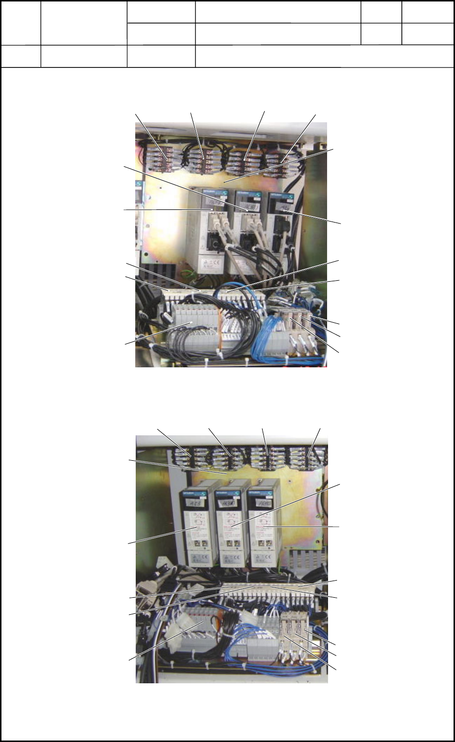
1.4 Layout of BA and BC Blocks
0406-001
13-5
A63 in Section A
A63 in Section B
A53
K49
K50
K40
K39
K60
K72
K71
K75
K76
K77
K78
(F021B to F024B)
(
F021A to F024A
)
R01A and R01B
behind Panel
Fig. M11 BA Block
A63 in Section D
A63 in Section C
A53
(F033~F036)
(F021D~F024D)
(F021C~F024C)
K75
K76
K77 K78
R01C and R01D
behind Panel
K40
K39
K49
K50
K60
K72
K71
Fig. M12 BC Block
Device
Name
Chip Mounter
Block Name
Page No.
Unit Name
Revision
Model ItemGXH-1
Chapter 13 Layout of Electrical
1. Layout of Underframe
Layout
Symbol Name
K39 Breaker (Backup Main Power Supply)
K40 Breaker (Backup Main Power Supply)
K49 Breaker (Cutter Power Supply in Section C)
K50 Breaker (Cutter Power Supply in Section D)
K60 Relay
K71 Relay
K72 Relay
K75 Relay (Feeder Power Supply)
K76 Relay (Feeder Power Supply)
K77 Relay (Feeder Power Supply)
K78 Relay (Feeder Power Supply)
A53 Backup Axis Amplifier
A63 Cutter Axis Amplifier
F021A to F024A Fuse (Feeder Power Supply)
F021B to F024B Fuse (Feeder Power Supply)
F021C to F024C Fuse (Feeder Power Supply)
F021D to F024D Fuse (Feeder Power Supply)
F033 to F036 Fuse
R01A Resistor
R01B Resistor
R01C Resistor
R01D Resistor
0406-001
13-6
Device
Name
Chip Mounter
Block Name
Page No.
Unit Name
Revision
Model ItemGXH-1
Chapter 13 Layout of Electrical
1. Layout of Underframe
Layout
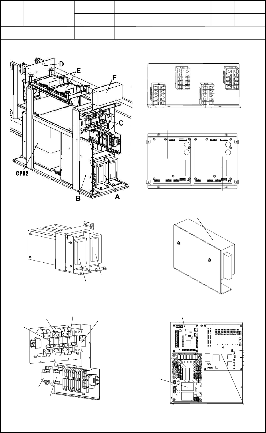
1.5 Layout of BL Blocks
K29
K28
Q
206
Q
205
Q
203
Q
204
UA54
UB21
UB14
G02
G04
A51
A41
K38
K37
K36
K35
G05
Rear Side Front Side
Fig. M13 Whole View of BL Block
Fig. M14 Section D
Fig. M15 Section E
Fig. M16 Section A
Fig. M17 Section F
Fig. M18 Section C
Fig. M19 Section B
0406-001
13-7