SM-131-006.pdf - 第229页
Device Name Chip Mounter Block Name Page No. Unit Name Revision Model Item GXH-1 Chapter 13 Layout of Electrical 1. Layout of Underframe Layout 1.8 Layout of FB Blocks Symbol Name U82 Motion Control Board U83 Motion Cont…
Device
Name
Chip Mounter
Block Name
Page No.
Unit Name
Revision
Model ItemGXH-1
Chapter 13 Layout of Electrical
1. Layout of Underframe
Layout
1.7 Layout of FA Blocks
0406-001
13-11
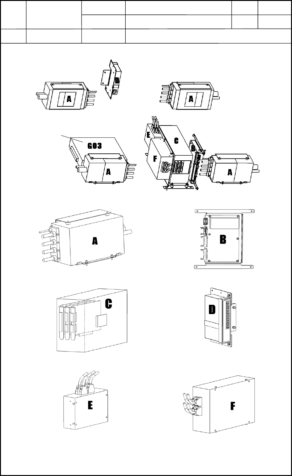
Fig. M28 Lighting for Component Recognition
Fig. M30 Recognition Box
Fig. M32 Selector
Fig. M31 Hub
Fig. M33 CPU1
DC Power Supply
Fig. M27 Whole Component Recognition Lighting in FA Block
Fig. M29 Lighting Control Board
UB08
Device
Name
Chip Mounter
Block Name
Page No.
Unit Name
Revision
Model ItemGXH-1
Chapter 13 Layout of Electrical
1. Layout of Underframe
Layout
1.8 Layout of FB Blocks
Symbol Name
U82 Motion Control Board
U83 Motion Control Board
U84 Motion Control Board
0406-001
13-12
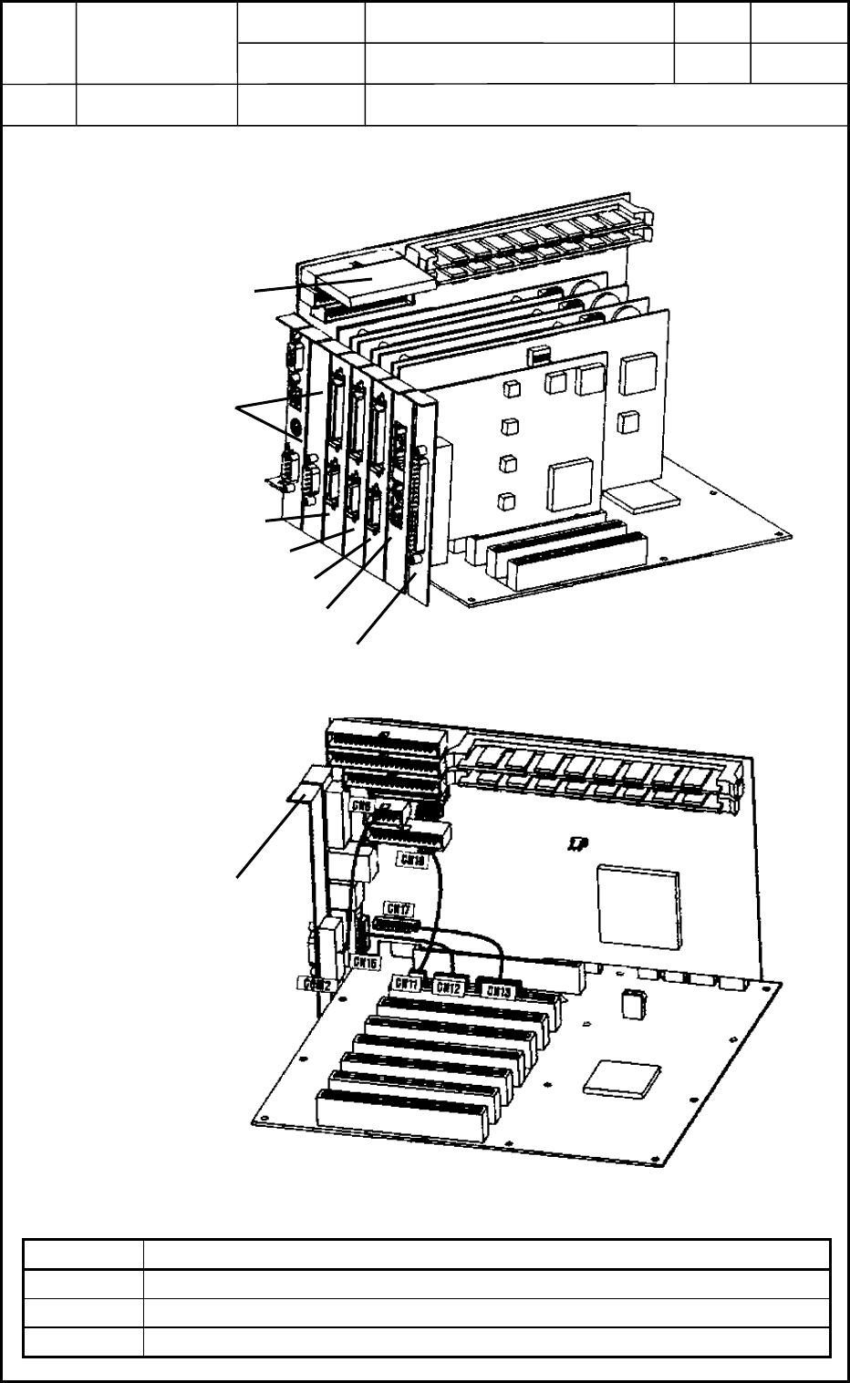
Memory Card
CPU Board
U82
U83
U84
HLS Centerboard
SERIAL Communication Board
Fig. M34 Internal View of CPU2
CPU Board
COM2 Pullout Panel
Back Plane
Fig. M35 Internal Connections of CPU2
Device
Name
Chip Mounter
Block Name
Page No.
Unit Name
Revision
Model ItemGXH-1
Chapter 13 Layout of Electrical
1. Layout of Underframe
Layout
1.9 Layout of BF Blocks
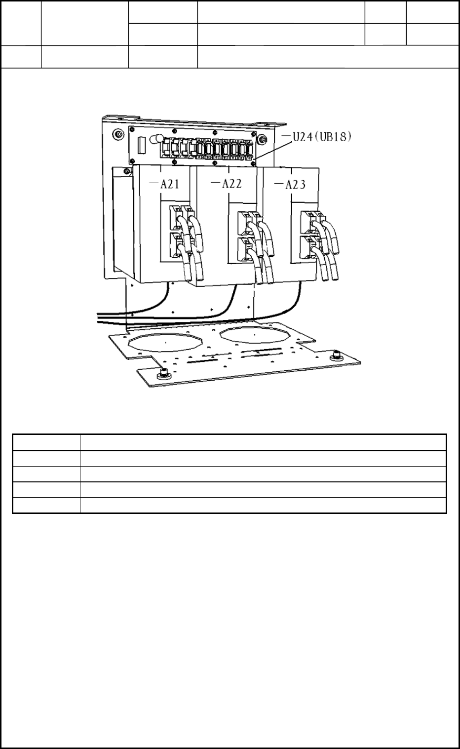
Symbol Name
A21 X-Axis Servoamplifier
A22 Y1-Axis Servoamplifier
A23 Y2-Axis Servoamplifier
U24 Beam Relay Board UB18
0406-001
13-13
Fig. M36 Arrangement of Beam Amplifiers