00190802-02.pdf - 第234页
8 Product / PCB User’s Manual Line Computer UNIX 8.1 PCB Editor Software Version 402.xx Edition 06/ 96 8 - 16 Fig. 8.1.7 "Graphic Mode" displa y with additional struc ture graphic ☞ NO TE per taining to Fig. 8.…
User’s Manual Line Computer UNIX 8 Product / PCB
Software Version 402.xx Edition 06/96 8.1 PCB Editor
8 - 15
8.1.3.4 Setting Area of Structure Editor (Graphic Mode)
-
For a better visualization of the PCB in the display area, a zoom factor (10 - 999%) can be entered in the
editing field of the setting area, with the factor "100" corresponding to reality.
-
The remaining display options are symbolized by icons (see Fig. 8.1.6). The desired setting can be achie-
ved by activating an icon (see the description below).
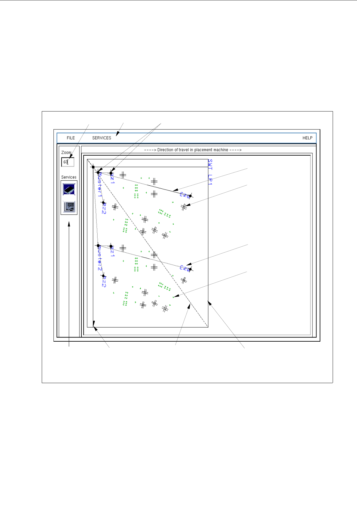
Fig. 8.1.6 Main Window "Structure Editor" ("Graphic Mode" Display)
setting area
menu bar
placement position
fiducial
offset vector
x-axis (+)
editing field PCB zero points
PCB
dimensional vectors
Outline (dimensions)
of the PCB
name of the PCB
substructure
8 Product / PCB User’s Manual Line Computer UNIX
8.1 PCB Editor Software Version 402.xx Edition 06/96
8 - 16
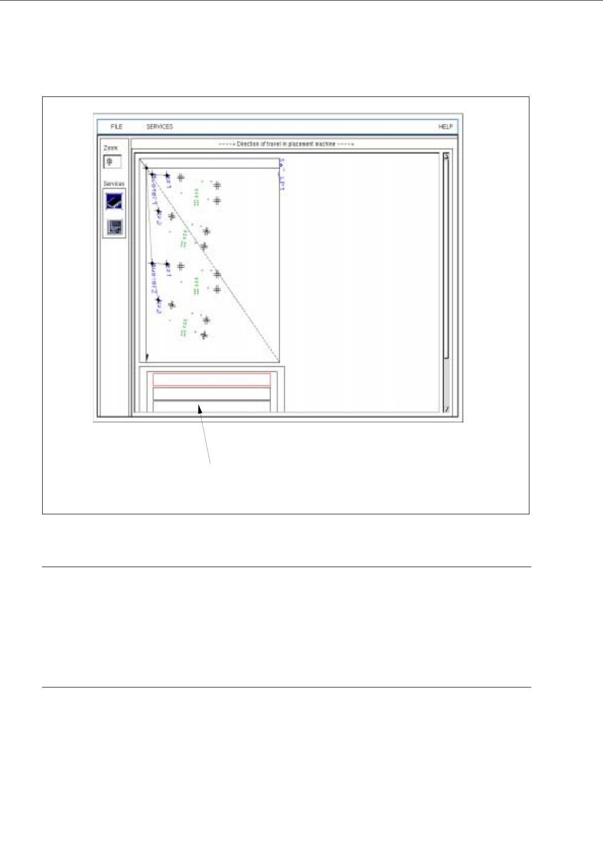
Fig. 8.1.7 "Graphic Mode" display with additional structure graphic
☞
NOTE
pertaining to Fig. 8.1.7
The Structure Graphic symbolically represents the overall structure of the PCB and is only created for those
PCBs with at least one substructure whose offset values are not completely defined. The Structure Graphic
does not provide any geometrical information about the substructure, but rather merely reveals the interrelation-
ships of the substructures as well as the status of the offset data of the substructures. In the Structure Graphic
the substructures are represented as rectangles of different colors.
The meaning of the colors is described in section 8.1.3.7.
Structure Graphic
(is only displayed if the offset values are not completely defined)
User’s Manual Line Computer UNIX 8 Product / PCB
Software Version 402.xx Edition 06/96 8.1 PCB Editor
8 - 17
Settings:
-
Setting the zoom factor
●
Click on the editing field and enter the desired value (10 to 999).
●
To accept the entry, press the RETURN key.
The PCB is displayed in the desired size.
-
Turning the placement position display on/off
This option serves to toggle the display of the placement positions (PPs) to the on or off state. By
default, the display of the PPs is turned on.
●
Click on icon .
If the display of the PPs was turned on, the PPs are no longer displayed now, and the icon is mar-
ked by a red cross.
-
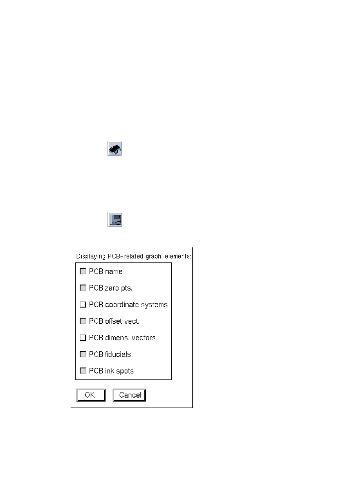
Selecting display options
To obtain a clearly arranged display of the PCB, the respectively required graphical elements can be
selected individually (e.g. only the display of the PCB fiducials).
●
Click on icon .
The following dialog box is opened:
●
Activate or deactivate the desired display options (graphical elements) by clicking on the
respective buttons.
●
Click on
OK
.
The dialog box is closed, and the PCB with the selected graphical elements is displayed in the
display area (see Fig. 8.1.6).