00190802-02.pdf - 第518页
17.2 Description of Components and PCBs User’s Manual SIPLACE Line Com puter UNIX 17.2.2 PCB 2: F ocus on P ackage F or m Description Software V ersion 402.xx Edition 06/ 96 17 - 18 Package fo rm description for pa ckage…
User’s Manual SIPLACE Line Computer UNIX 17.2 Description of Components and PCBs
Software Version 402.xx Edition 06/96 17.2.2 PCB 2: Focus on Package Form Description
17 - 17
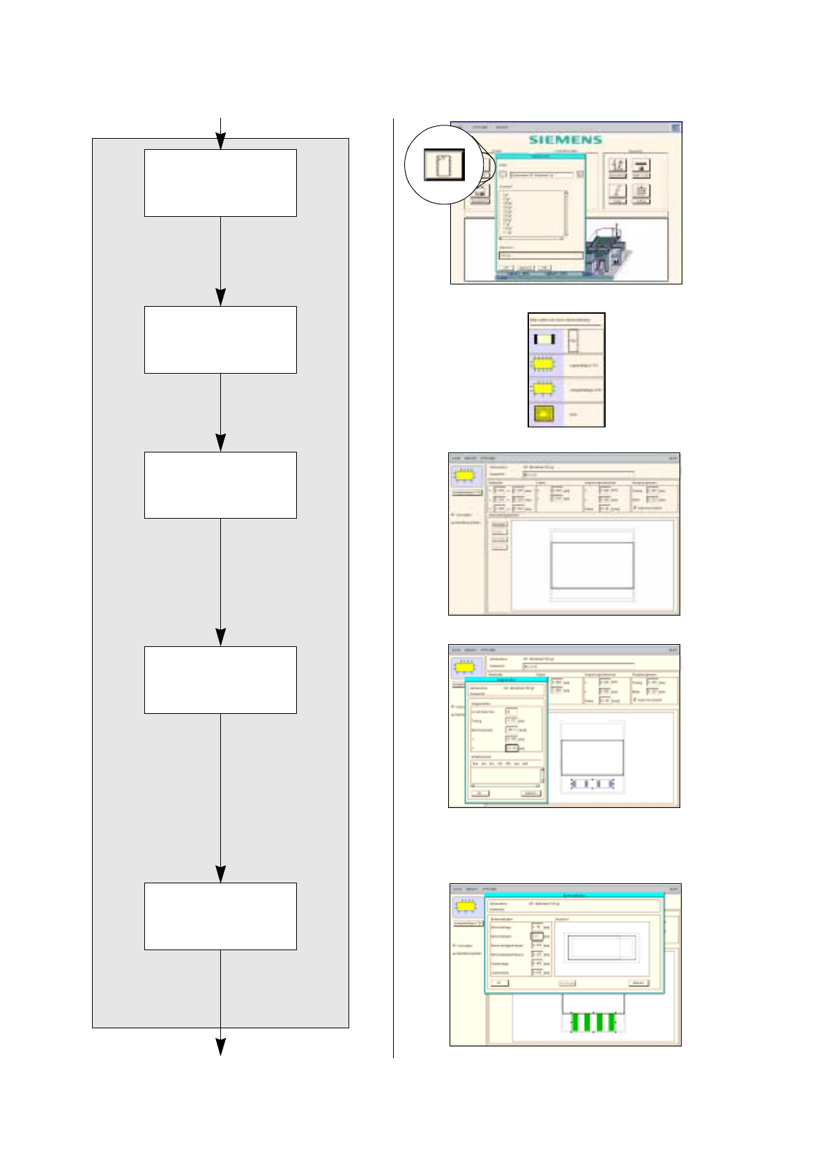
To define the pin model for package form 1502, proceed as follows:
38. Select one of the two pin groups by clicking on it.
39. Click on the
Pin/Ball
button.
The Pin model data window is opened.
40. Enter the pin model data,
confirm by pressing the Enter key, here:see chart:
The automatically calculated values of the other editing fields can be adopted.
Every time the Enter key is pressed, the display of the pin model is updated.
41. Click on the
OK
button.
The Pin model data window is closed. The package form with pins is displayed.
To enter the handling data for package form 1502, proceed as follows:
42. Activate the
Handling data
button.
The selection areas are displayed for entering the handling data.
43. In the Nozzles/Sensor types selection area activate the
Nozzle
button.
44. Click on the
Create
button.
The Nozzle type selection window containing a list of the nozzle types is loaded.
45. Click on a nozzle, here:
416
.
The selection window is closed, the nozzle is accepted.
46. Activate the
Sensor type
button.
47. Click on the
Create
button.
The Sensor type selection window containing a list of the sensor types is opened.
48. Click on a sensor type, here:
7
.
The selection window is closed, the sensor type is accepted.
49. Enter the appropriate value in the
Placing force
editing field in the Handling values selection area,
here:
2
.
50. Activate the appropriate button in the Centering selection area, here:
External centering
.
51. In this example the default values of the editing areas Handling instructions and Reduced acceleration
can be adopted, no entries are required.
To allocate a feeder to package form 1502:
52. Click on the
Starting Feeder Editor
option on the
SERVICES
menu.
The Feeder Editor is opened.
53. Activate the
Allocate
icon .
54. Activate a button for the line or a feeder part, here:
Line
.
The entire line is highlighted in light-green.
55. Click on the appropriate feeder on the list of placeable feeders, here:
FD~S_G_32_III
.
The feeder is transferred to the Feeder selection field.
56. In the Feeder Editor click on the
Save
option on the
FILE
menu.
The data are now saved.
57. Click on the
Quit
option on the
FILE
menu.
The Feeder Editor is closed.
58. In the Package Form Editor click on the
Save
option on the
FILE
menu.
The data are now saved.
59. Click on the
Quit
option on the
FILE
menu.
The Package Form Editor is closed.
Pin length L
1
Pin width b
0.8 0.2
17.2 Description of Components and PCBs User’s Manual SIPLACE Line Computer UNIX
17.2.2 PCB 2: Focus on Package Form Description Software Version 402.xx Edition 06/96
17 - 18
Package form description for package form 1503
continued from page 17-16
continued on page 17-20
Defining pin model
Entering dimensions
Defining package
form type for package
form 1503
Creating pin group
Opening Package
Form Editor for
package form 1503
User’s Manual SIPLACE Line Computer UNIX 17.2 Description of Components and PCBs
Software Version 402.xx Edition 06/96 17.2.2 PCB 2: Focus on Package Form Description
17 - 19
C) Description of an irregular FDC using package form 1503 as an example
To open the Package Form Editor for package form 1503, proceed as follows:
60. On the desktop click on the icon of the Package Form Editor .
The file selection window is opened.
61. Click on the
Selection
editing field.
62. Enter the package form number, here:
1503.gf
and click on the
OK
button.
The Package Form Editor with the Package form type selection window is opened.
To define the package form type „irregular FDC“ for package form 1503, proceed as follows:
63. Click on the
Irregular FDC
type in the Package form type selection window.
The selection window is closed.
64. In the Package Form Editor click on the
Comment
editing field, enter a unique comment, here:
Micro-X
.
To enter the dimensions for package form 1503, proceed as follows:
65. Enter the dimensions of the package form with pins in the Nominal dimensions editing area, confirm your
entry by pressing the Enter key, here: see chart:
The tolerances are entered automatically.
The package form with the tolerance range is displayed.
66. Enter the dimensions of the package form without pins in the Body editing area, confirm by pressing the
Enter key, here: see chart:
(These entries are only required for the display).
The display of the package form is updated.
67. In this example the default values of the Packaging tolerances and Features editing areas can be
adopted, no entries are required.
To create the lower pin group (pins 1 to 4) of package form 1503, proceed as follows:
68. Click on the
Create
button.
The Group data window is opened. On the upper side of the component a predefined pin group with three
pins (gray areas) is displayed.
69. Overwrite the default values in the editing fields with the pin group data for package form 1503 (see dis-
plays in On-line Help) and confirm your entry by pressing Enter key, here: see chart:
Every time the Enter key is pressed, the display of the pin group (gray areas) is updated, the pin groups
are now displayed on the bottom side of the component.
70. Click on the
OK
button.
The Group data window is closed.
To define the pin model for the lower pin group of package form 1503, proceed as follows:
71. Select one of the two pin groups by clicking on it.
72. Click on the
Pin/Ball
button.
The Pin model data window is opened.
73. Enter the pin model data, here: see chart:
In this example the automatically calculated values of the other editing fields can be adopted. Every time
the Enter key is pressed, the display of the pin model is updated.
74. Click on the
OK
button.
The Pin model data window is closed. The package form together with the pins is displayed at the
bottom side.
X
(Length D)
Y
(Width H
E
)
Z
(Height A)
6.5 7 1.8
X
(Length D)
Y
(Width E)
6.5 3.5
No. of pins
Spacing
e2
Pin angle
X (BG
Off
) Y (BG
Off
)
4 1.27 -90 0 -2.625
Pin length BL Pin width b
1.75 0.6