00190802-02.pdf - 第528页
17.2 Description of Components and PCBs User’s Manual SIPLACE Line Com puter UNIX 17.2.2 PCB 2: F ocus on P ackage F or m Description Software V ersion 402.xx Edition 06/ 96 17 - 28 No clusters and sin gle circ uits are …
User’s Manual SIPLACE Line Computer UNIX 17.2 Description of Components and PCBs
Software Version 402.xx Edition 06/96 17.2.2 PCB 2: Focus on Package Form Description
17 - 27
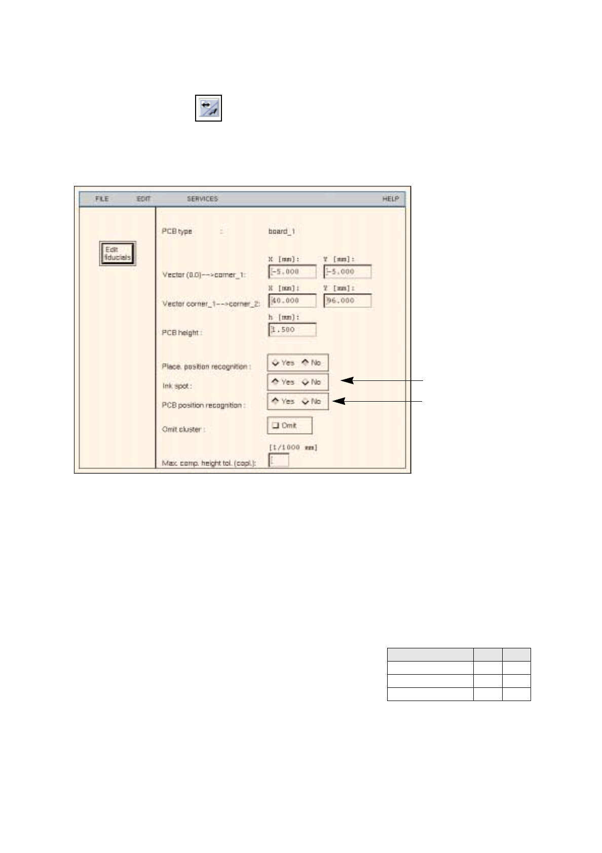
To enter the dimensional data of the PCB, proceed as follows:
135.Click on the Menu icon .
136.Click on the PCB (rectangle).
137.Click on the
Cluster Editor
option on the
SERVICES
menu.
The Cluster Editor is opened.
138.Enter the dimensions of the PCB. See Fig. 17.2.4 on pages 17-10 and Fig. 17.2.5 .
Fig. 17.2.5 Cluster Editor for PCB 2
To define the fiducials, proceed as follows:
139.In the Cluster Editor click on the
Edit fiducials
button.
The Fiducial Editor is opened.
140.Activate the
Insert
button.
141.Click on the
Fiducial set name
editing field.
142.Enter a name for the new fiducial set, here:
Set_1
.
143.Click on the
Accept fiducial set
button.
The fiducial set Set_1
appears on the fiducial list.
144.Click on fiducial set Set_1 on the fiducial list.
145.Click on the
Fiducial
editing field.
146.Enter the fiducial number for the first fiducial, here:
48
.
147.Click on the editing fields for the coordinates, enter coordinates
(do not confirm with Enter key!), here: see chart:
148.Click on the
Accept fiducial data
button.
The data of the fiducial are transferred to the list of the fiducials of the fiducial set.
149.Define the remaining fiducials accordingly, here:
fiducials
48
and
48
.
150.Activate the
PCB position recognition
button.
151.Click on the fiducial set Set_1 on the fiducial list.
The fiducial set
Set_1
is marked by a preceeding
L
for PCB position recognition.
Fiducial number X Y
48 30 0
48 0 86
48 30 86
Activate ink spot
Activate PCB pos. recognition
17.2 Description of Components and PCBs User’s Manual SIPLACE Line Computer UNIX
17.2.2 PCB 2: Focus on Package Form Description Software Version 402.xx Edition 06/96
17 - 28
No clusters and single circuits are present.
FILE
Save
FILE
Quit
Saving PCB data
continued from page 17-26
Entering placement
positions
Defining ink spot
Creating clusters and
single circuits
PCB description

User’s Manual SIPLACE Line Computer UNIX 17.2 Description of Components and PCBs
Software Version 402.xx Edition 06/96 17.2.2 PCB 2: Focus on Package Form Description
17 - 29
To define the ink spot, proceed as follows:
152.In the Fiducial Editor activate the
Insert
button.
153.Click on the
Fiducial set name
editing field.
154.Enter a name for the new fiducial set (ink spot), here:
ink
.
155.Click on the
Accept fiducial set
button.
The ink fiducial set appears on the fiducial list.
156.Click on the ink fiducial set on the fiducial list.
157.Click on the
Fiducial
editing field.
158.Enter the fiducial number, here:
48
.
159.Click on the individual editing fields for the coordinetes and enter
the coordinates (do not confirm with the Enter key), here: see chart:
160.Click on the
Accept fiducial data
button.
The data of the ink spot are transferred to the list of the fiducials of the fiducial set.
161.Activate the
Ink spot fiducial set
button.
162.Click on the ink fiducial set on the fiducial list.
The ink fiducial set name is preceded by an
I
for ink spot.
163.Click on the
Quit
option on the
FILE
menu.
The Fiducial Editor is closed.
164.In the Cluster Editor click on the
Quit
option on the
FILE
menu.
The Cluster Editor is closed.
To create clusters and single circuits, proceed as follows:
no clusters and single circuits are present.
To enter the placement positions, proceed as follows:
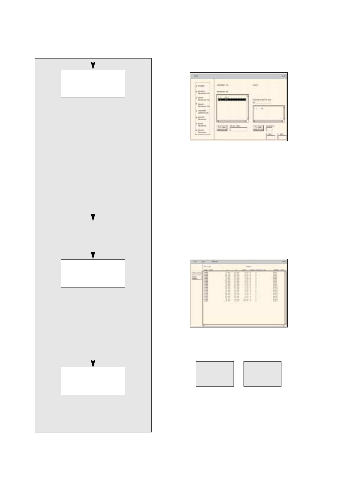
165.In the Component Editor click on the Menu icon.
166.Click on the PCB (rectangle).
167.Click on the
Placement Position Editor
option on the
SERVICES
menu.
The Placement Position Editor is opened.
168.Position the cursor in the entry field and enter the placement positions in accordance with Charge 17.2-3
on page 17-10. The individual entries are to be separated by a blank. Every line is to be confirmed by
pressing the Enter key. See also Fig. 17.2.6 on page 17-30.
169.When the entry has been completed, click on the
Check PP
button.
The values entered are checked and arranged in columns.
170.Click on the
Quit
option on the
FILE
option.
The Placement Position Editor is closed.
To save the PCB data, proceed as follows:
171.In the PCB Editor click on the
Save
option on the
FILE
menu.
The PCB data are saved.
172.Click on the
Quit
option on the
FILE
menu.
The PCB Editor is closed. The description of PCB 2 is terminated.
Fiducial number X Y
48 15 0