slau358q.pdf - 第133页
www.ti.com Schematics 133 SLAU358Q – September 2011 – Revised October 2019 Submit Documentation Feedback Copyright © 2011–2019, Texas Instruments Incorporated Schematics Figure 5-7. Schematic of MSP-GANG 14-20 Adapter NO…
Schematics
www.ti.com
132
SLAU358Q–September 2011–Revised October 2019
Submit Documentation Feedback
Copyright © 2011–2019, Texas Instruments Incorporated
Schematics
Table 5-1. Gang Splitter Bill of Materials (BOM)
Item Name Drawing and Part Number Quantity Description
1 BLANK PC BOARD MSP-GANG-SP rev-2 1 Blank PC Board
THROUGH HOLE COMPONENTS
1 Connector SBH11-PBPC-D07-ST-BK 1 14-pins Header Connector (Sullins)
2 Connector SBH11-PBPC-D07-ST-BK 1 14-pins Header Connector (Sullins)
3 Connector SBH11-PBPC-D07-ST-BK 1 14-pins Header Connector (Sullins)
4 Connector SBH11-PBPC-D07-ST-BK 1 14-pins Header Connector (Sullins)
5 Connector SBH11-PBPC-D07-ST-BK 1 14-pins Header Connector (Sullins)
6 Connector SBH11-PBPC-D07-ST-BK 1 14-pins Header Connector (Sullins)
7 Connector SBH11-PBPC-D07-ST-BK 1 14-pins Header Connector (Sullins)
8 Connector SBH11-PBPC-D07-ST-BK 1 14-pins Header Connector (Sullins)
J9 Connector TX24-100R-LT-H1E 1
100p-Receptacle Right Angle Connector (JAE
Electronics)
J10 Connector do not populate 2-pins terminal block
Bumpers SJ61A6 3 Bumpon, cylindrical 0.312 x 0.215, black
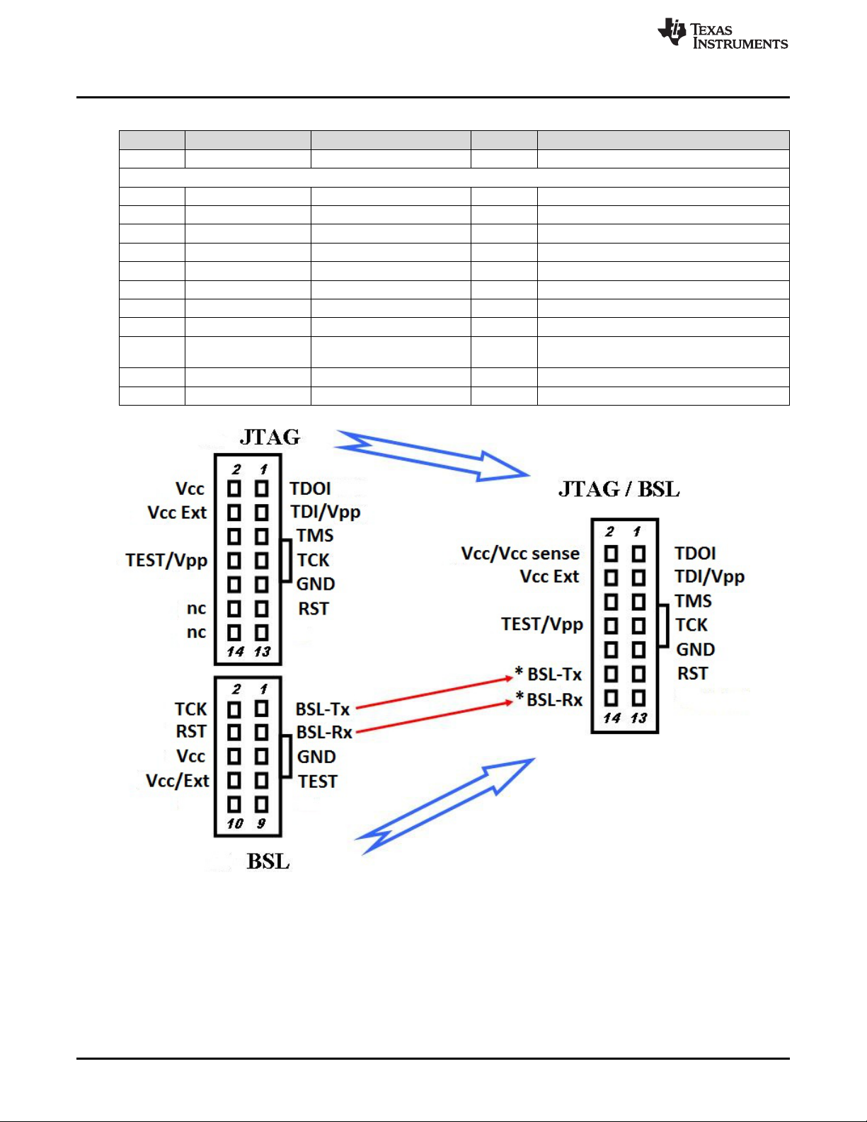
Figure 5-6. BSL Connection Schematic
Detailed description of the BSL connection can be found in MSP430 Programming With the Bootloader
(BSL) (SLAU319). It is important to note that the MSP-GANG Programmer's Fast-BSL has much higher
communication speed than standard BSL, 200 kbps compared to 9.6 kbps. Consequently, ensure that the
hardware does not have additional delay on the BSL RX and TX lines beyond 0.5 µs (a clock pulse
duration of 2 µs must be transmitted by the BSL RX and TX lines without degradation). Any additional
filters or suppressors on the BSL RX and TX lines can degrade communication.
www.ti.com
Schematics
133
SLAU358Q–September 2011–Revised October 2019
Submit Documentation Feedback
Copyright © 2011–2019, Texas Instruments Incorporated
Schematics
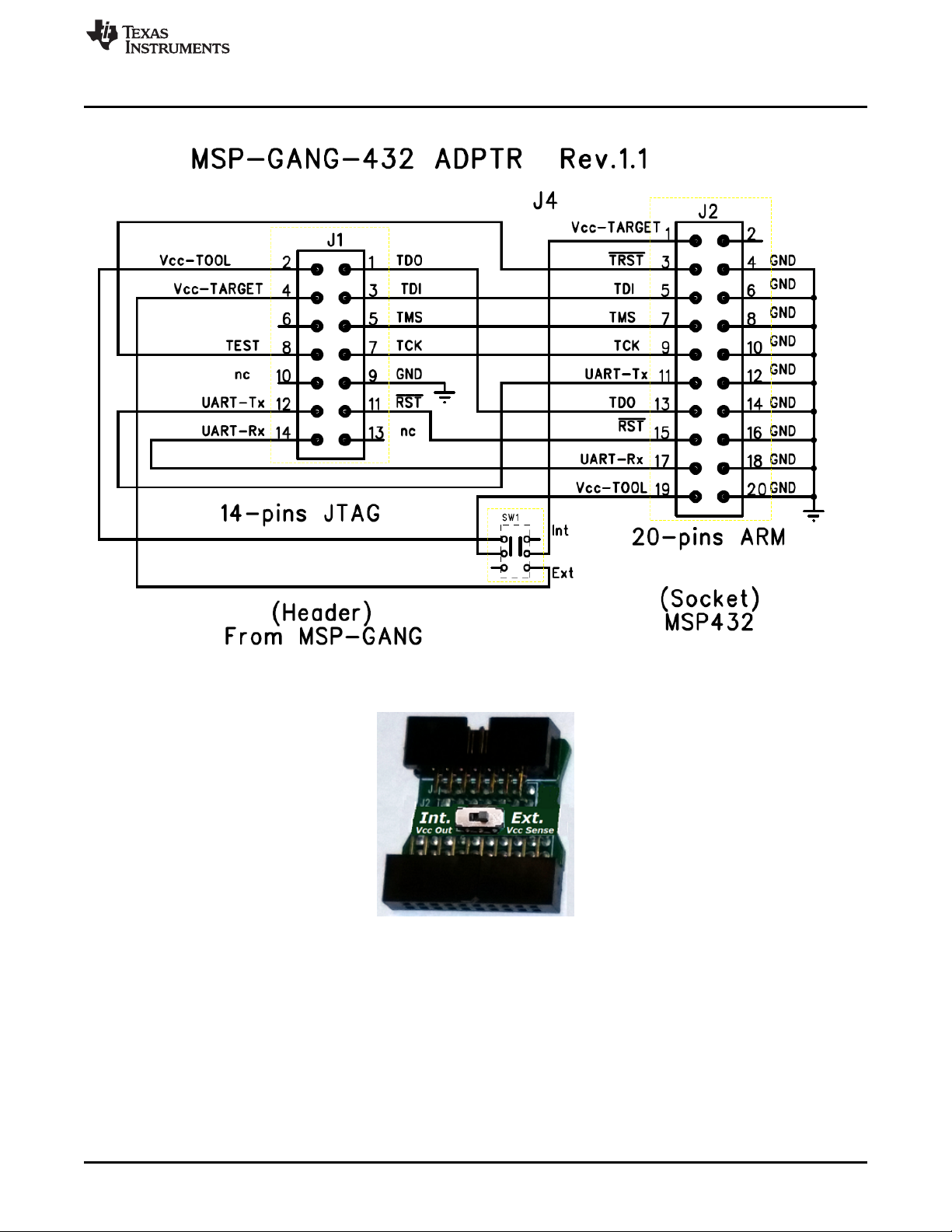
Figure 5-7. Schematic of MSP-GANG 14-20 Adapter
NOTE: Adapter should be plugged in on the 14-pin JTAG cable. The 20-pin end is connected to the MSP432
JTAG connector on the target board.
Figure 5-8. Top View of MSP-GANG 14-20 Adapter (Order Separately From TI)

134
SLAU358Q–September 2011–Revised October 2019
Submit Documentation Feedback
Copyright © 2011–2019, Texas Instruments Incorporated
Frequently Asked Questions
Chapter 6
SLAU358Q– September 2011 –Revised October 2019
Frequently Asked Questions
6.1 Question: Why does device init, connect, or programming fail?
Answer: Frequently the cause is a bad connection between the MSP-GANG Programmer and the target
device. A 14-wire ribbon cable is provided for JTAG/SBW or BSL connection between MSP-GANG and
target device. The ribbon cable has an impedance of approximately 100 Ω and has DC lines in the ribbon
cable to provide good isolation between signal wires (TDI, TCK, TMS, TDO). Each signal wire is
separated by a DC wire to minimize crosstalk between the signal wires. The following pinout used in the
MSP-GANG on each JTAG connector:
1 - TDO (Signal wire)
2 - Vcc / Vcc sense (DC wire)
3 - TDI (Signal wire)
4 - Vcc sense (DC wire)
5 - TMS (Signal wire)
6 - n/c (DC wire)
7 - TCK (Signal wire)
8 - TEST (DC wire in JTAG)
9 - GND (DC wire)
10 - n/c (DC wire)
11 - RESET (DC wire in JTAG)
12 - BSL-Tx (Signal wire)
13 - n/c (DC wire)
14 - BSL-Rx (Signal wire)
The provided 14-pin connector might not be ideal for some customers who want to minimize the number
of wires and pinout order. When using a custom cable, make sure to address the issue of crosstalk
between signal cables. Unfortunately, in many cases the custom cable does not provide good isolation
between signal wires. As an example of a bad connection, the following uses an 8-wire ribbon cable for
JTAG communication:
1 - Vcc / Vcc sense (DC wire)
2 - TDO (Signal wire)
3 - TDI (Signal wire)
4 - TMS (Signal wire)
5 - TCK (Signal wire)
6 - TEST (DC wire in JTAG)
7 - GND (DC wire)
8 - RESET (DC wire in JTAG)
On this connection, the TMS signal is coupled with the TCK and TDI lines and can generate additional
TCK pulses on the TCK wire (rise time on TMS line can be seen on the TCK line also and can be
detected by the MSP MCU as an additional unexpected TCK pulse).