slau358q.pdf - 第16页
Programming MSP Flash Devices Using the MSP Gang Programmer www.ti.com 16 SLAU358Q – September 2011 – Revised October 2019 Submit Documentation Feedback Copyright © 2011–2019, Texas Instruments Incorporated Operation NOT…

www.ti.com
Programming MSP Flash Devices Using the MSP Gang Programmer
15
SLAU358Q–September 2011–Revised October 2019
Submit Documentation Feedback
Copyright © 2011–2019, Texas Instruments Incorporated
Operation
detected, a warning appears; however, if programming proceeds without changes the second code file
overwrites the conflict area. Code size and checksum appear on the right side.
5. Some MCUs (for example, the MSP430FR57xx) provide a method of disabling JTAG by programming
a password to flash memory. The password should be specified as data to be programmed starting at
0xFF80 and up to 0xFFFF (where 0xFF80 must be 0xAAAA, 0xFF82 must be the size of the password
in words, and 0xFF88-0xFFFF contains the password). The code file must contain password contents
if you intend to lock JTAG using the password feature after programming. If the MCU is already locked
using a previously programmed code file, then you must provide the password section (or entire old
code file) using the Open Password File button if and only if the password section is different.
Functionally, if the MCU is locked by password, the code file’s password section is first used to attempt
to unlock the MCU. If that fails, then the password file’s contents are used to attempt to unlock the
MCU. If both attempts fail, the MCU remains locked and JTAG access fails. Password file contents are
not used to program the MCU.
6. In the Target power group, select the desired V
CC
voltage and select if the target is supplied from the
MSP Gang Programmer or from an external power supply. If targets are supplied by the programmer,
then select the maximum current used by each target, 30 mA or 50 mA.
7. In the Results group, select desired target devices to be programmed. After programming has
concluded, a green checkmark or lights appear for successful operations for each target.
8. In the Interface selector, choose the desired interface (JTAG, SBW, SWD, or BSL) and communication
speed (fast, medium, or slow).
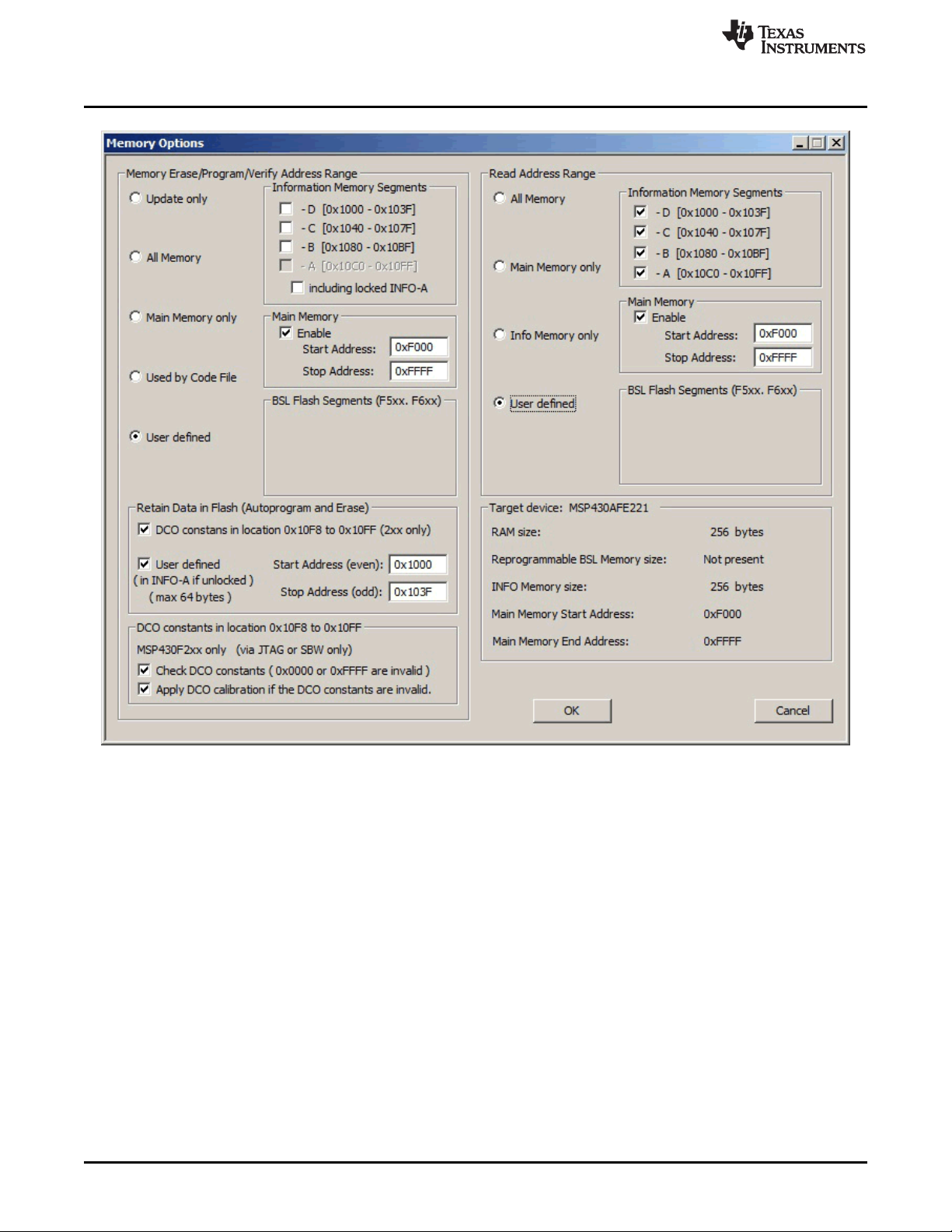
9. In the Memory Options dialog (pulldown menu: Setup→Memory options ) shown in Figure 2-2, select
desired memory space to be programmed. By default, the selected option is All Memory and it is
correct for most programming tasks (Section 2.1.5 describes how to use the memory configuration
window).
Programming MSP Flash Devices Using the MSP Gang Programmer
www.ti.com
16
SLAU358Q–September 2011–Revised October 2019
Submit Documentation Feedback
Copyright © 2011–2019, Texas Instruments Incorporated
Operation
NOTE: The user can select which segments of memory are written to or read from.
Figure 2-2. Memory Options
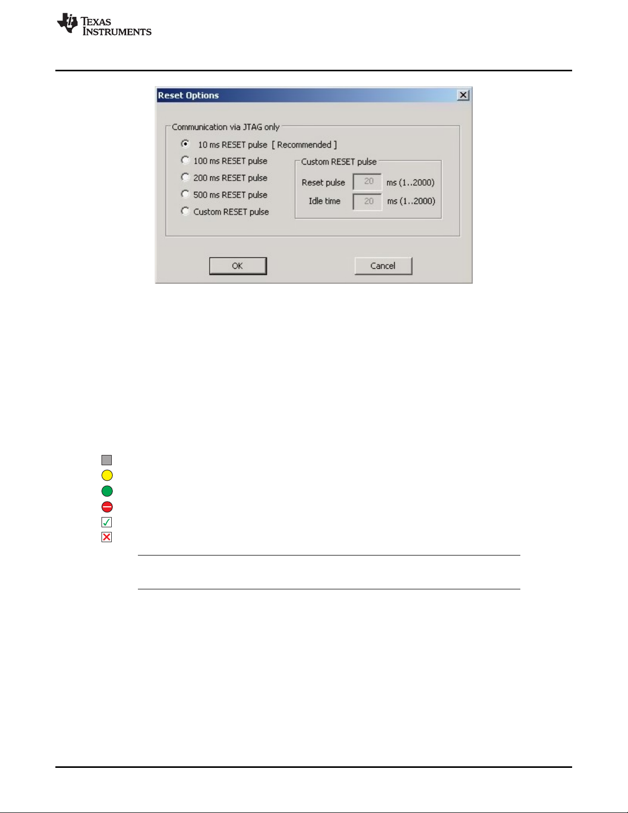
10. In the Reset Options dialog (pulldown menu: Setup→Device Reset ) shown in Figure 2-3, select the
duration of the reset pulse and the delay after reset. By default it is 10 ms, but other options are
available if required by the hardware.
www.ti.com
Programming MSP Flash Devices Using the MSP Gang Programmer
17
SLAU358Q–September 2011–Revised October 2019
Submit Documentation Feedback
Copyright © 2011–2019, Texas Instruments Incorporated
Operation
NOTE: This window lets the user specify the duration of the reset pulse coming from the MSP Gang Programmer
to the target device. Depending on the hardware implementation, a longer reset pulse might be required.
Figure 2-3. Reset Options
Following these steps creates a working setup that can program target devices using the MSP Gang
Programmer. Click the Save Project As button to save this configuration settings. These settings can be
loaded again later and modified, if necessary (one project holds one configuration). After saving the
project, use the buttons described in the following sections to perform the desired actions.
2.1.1.1 GO
Click the GO button in the Main Dialog GUI (or F9 key on the keyboard) to start programming. GO starts
erase, blank check, program, verify, or blow fuse if selected. The progress and completion of the operation
are displayed in the Results group. The result is shown as one of the following:
Idle status
Test in progress. For power on or off, DC voltage is correct.
Access enabled
Access denied (for example, the fuse is blown)
Device action has been finished successfully
Device action has been finished, but result failed
NOTE: When a FRAM MCU is selected, the blank check step is skipped. During global verification,
main code contents and empty values are verified.
2.1.1.2 Erase
Click the Erase button in the Main Dialog GUI to erase a segment of memory (sets each byte to 0xFF).
Use the Memory Options configuration screen shown in Figure 2-2 to specify which addresses should be
erased (Section 2.1.5 describes in detail how to use the memory configuration window). This action
succeeds after the programmer has attempted to erase the specified memory segment. Use the Blank
Check function to verify that this segment has been properly erased.