slau358q.pdf - 第17页
www.ti.com Programming MSP Flash Devices Using the MSP Gang Programmer 17 SLAU358Q – September 2011 – Revised October 2019 Submit Documentation Feedback Copyright © 2011–2019, Texas Instruments Incorporated Operation NOT…
Programming MSP Flash Devices Using the MSP Gang Programmer
www.ti.com
16
SLAU358Q–September 2011–Revised October 2019
Submit Documentation Feedback
Copyright © 2011–2019, Texas Instruments Incorporated
Operation
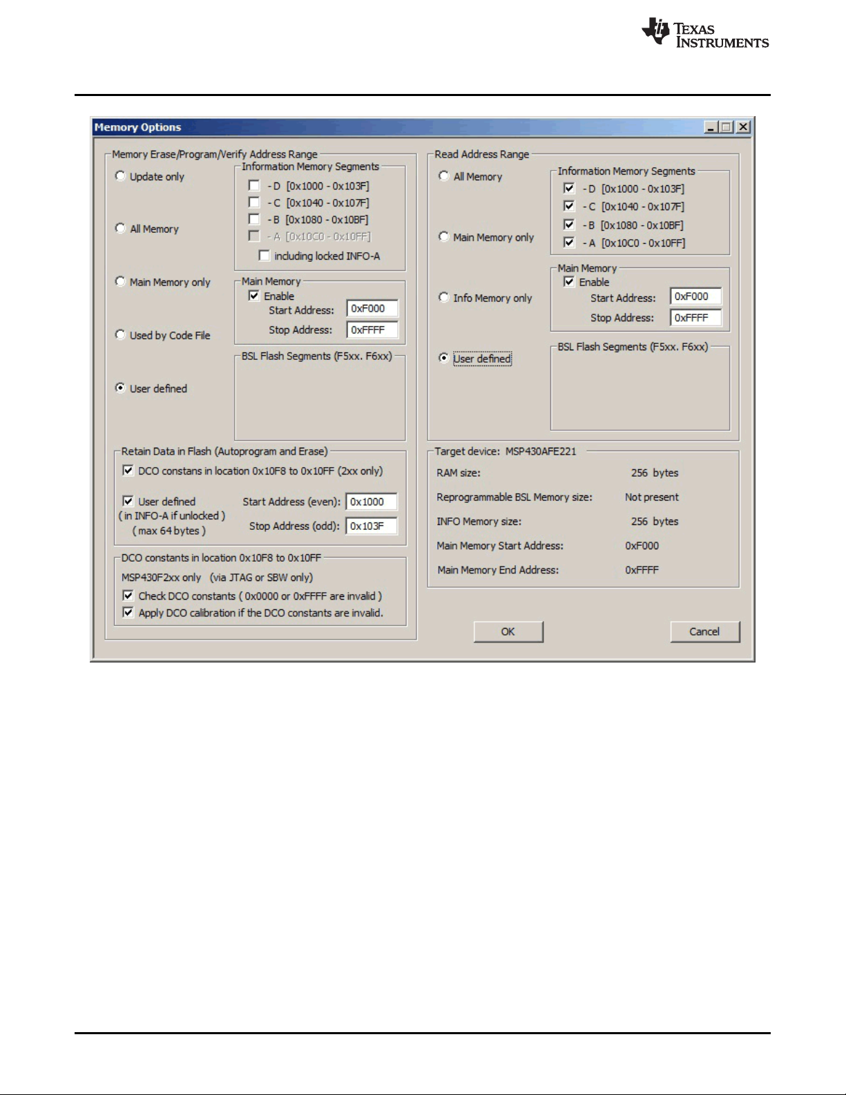
NOTE: The user can select which segments of memory are written to or read from.
Figure 2-2. Memory Options
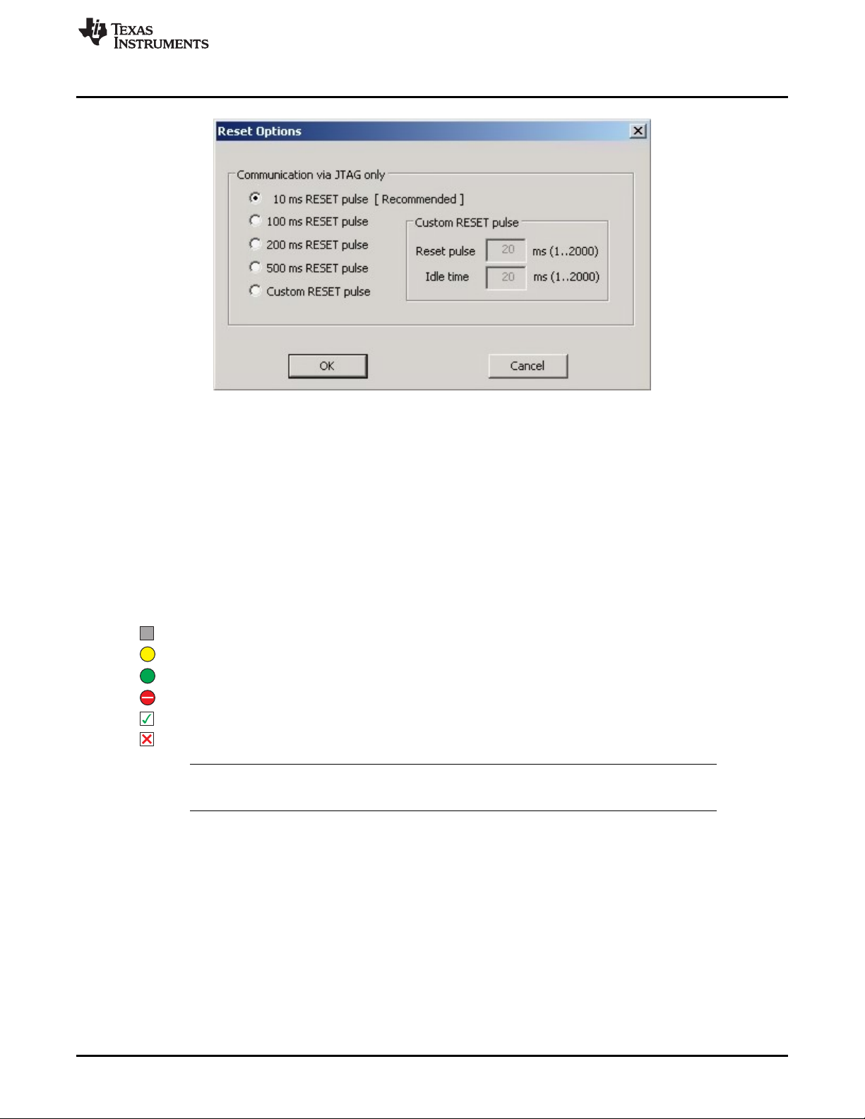
10. In the Reset Options dialog (pulldown menu: Setup→Device Reset ) shown in Figure 2-3, select the
duration of the reset pulse and the delay after reset. By default it is 10 ms, but other options are
available if required by the hardware.
www.ti.com
Programming MSP Flash Devices Using the MSP Gang Programmer
17
SLAU358Q–September 2011–Revised October 2019
Submit Documentation Feedback
Copyright © 2011–2019, Texas Instruments Incorporated
Operation
NOTE: This window lets the user specify the duration of the reset pulse coming from the MSP Gang Programmer
to the target device. Depending on the hardware implementation, a longer reset pulse might be required.
Figure 2-3. Reset Options
Following these steps creates a working setup that can program target devices using the MSP Gang
Programmer. Click the Save Project As button to save this configuration settings. These settings can be
loaded again later and modified, if necessary (one project holds one configuration). After saving the
project, use the buttons described in the following sections to perform the desired actions.
2.1.1.1 GO
Click the GO button in the Main Dialog GUI (or F9 key on the keyboard) to start programming. GO starts
erase, blank check, program, verify, or blow fuse if selected. The progress and completion of the operation
are displayed in the Results group. The result is shown as one of the following:
Idle status
Test in progress. For power on or off, DC voltage is correct.
Access enabled
Access denied (for example, the fuse is blown)
Device action has been finished successfully
Device action has been finished, but result failed
NOTE: When a FRAM MCU is selected, the blank check step is skipped. During global verification,
main code contents and empty values are verified.
2.1.1.2 Erase
Click the Erase button in the Main Dialog GUI to erase a segment of memory (sets each byte to 0xFF).
Use the Memory Options configuration screen shown in Figure 2-2 to specify which addresses should be
erased (Section 2.1.5 describes in detail how to use the memory configuration window). This action
succeeds after the programmer has attempted to erase the specified memory segment. Use the Blank
Check function to verify that this segment has been properly erased.

Programming MSP Flash Devices Using the MSP Gang Programmer
www.ti.com
18
SLAU358Q–September 2011–Revised October 2019
Submit Documentation Feedback
Copyright © 2011–2019, Texas Instruments Incorporated
Operation
2.1.1.3 Blank Check
Click the Blank Check button in the Main Dialog GUI to check that the contents of specified memory have
been properly erased. This function is best used after erasing the same segment of memory, using the
button described above. Use the same Memory Options configuration screen shown in Figure 2-2 to
specify which addresses should be erased (Section 2.1.5 describes in detail how to use the memory
configuration window). This function succeeds when the specified memory segments are set to 0xFF, and
fails otherwise.
2.1.1.4 Program
Click the Program button in the Main Dialog GUI to write the contents of a code files to flash memory on
the target device. Addresses specified in the code files are used to determine where the program is
written. Make sure that the regions of memory corresponding to the addresses in the code file are enabled
for writing in the Memory Options configuration screen shown in Figure 2-2 (Section 2.1.5 describes in
detail how to use the memory configuration window).
Configuration conflicts may arise during programming. It is possible that the code the user has chosen is
too big to fit in the flash memory of the target MCU, or the appropriate memory segments have not been
enabled in the Memory Options configuration screen. If this is the case, a warning message appears to
notify the user of insufficient memory; however, the user is still allowed to proceed. If the user proceeds
despite the warning, only the portion of code that fits within the MCU's enabled flash memory is written.
This function succeeds after the programmer has attempted to write code to the specified memory
addresses. Use the Verify function to ensure that the code has been correctly copied to flash on the target
MCU.
2.1.1.5 Verify
Click the Verify button in the Main Dialog GUI to verify that the contents of the target MCU's flash memory
have been properly programmed. This function is best used after programming the same segment of
memory, as performed using the button described above. Make sure that the same memory segments are
enabled in the Memory Options configuration window shown in Figure 2-2, as during programming
described above, to ensure all programmed segments are verified (Section 2.1.5 describes in detail how
to use the memory configuration window).
Verification of selected flash memory is divided into two steps: (1) verify selected flash memory that only
corresponds to the code file, and (2) verify selected flash memory that corresponds to the code file AND
selected flash memory not included in the code file that should be empty (0xFF). Examples of selected
flash memory include Main Memory, All Memory, or User defined, with the exception of Retain Data (if
defined). Verified flash memory that only corresponds to the code file is displayed in the GUI using Verify-
XXXX messages, where XXXX is the start address of a contiguous code segment. Verified flash memory
that corresponds to the code file AND flash memory not included in the code file is displayed in the GUI
using Gl.Verify-XXXX messages; where XXXX is the start address of a contiguous code and empty data
segment. Each contiguous segment is verified using a checksum (CS) and pseudo-signature analysis
(PSA). Verification passes if the CS and PSA match between flash memory and the code file.
If configuration conflicts arose during programming that indicated that the MCU did not contain sufficient
memory for the code to be programmed (either enabled segments or total memory was too small), then
the Verify function verifies only the code that was programmed and ignores the code that could not fit in
memory. This function succeeds if the code in flash matches the code file, and fails otherwise.
If the verification fails for any reason, TI recommends using an option from the pulldown menu
View→Compare Code File and Flash Data. When this option is enabled, the contents of the Flash or
FRAM memory is read and compared with used code file contents. Only bytes defined in the Code File
contents are compared. All other byte contents taken from the Flash or FRAM are ignored, regardless of
their content. If no errors are found by this verification, even the verification itself failed, then bytes outside
of the code file (not programmed) have a value other than 0xFF. Check the firmware that was downloaded
to Flash or FRAM to determine if the firmware is modifying the Flash or FRAM in unused memory space
after MCU reset (for example, if the Flash or FRAM is used for additional memory space like EEPROM).
If the verification fails and the MCU has FRAM memory, then the following pop-up message is displayed.