slau358q.pdf - 第33页
www.ti.com Programming MSP Flash Devices Using the MSP Gang Programmer 33 SLAU358Q – September 2011 – Revised October 2019 Submit Documentation Feedback Copyright © 2011–2019, Texas Instruments Incorporated Operation 2.1…
Programming MSP Flash Devices Using the MSP Gang Programmer
www.ti.com
32
SLAU358Q–September 2011–Revised October 2019
Submit Documentation Feedback
Copyright © 2011–2019, Texas Instruments Incorporated
Operation
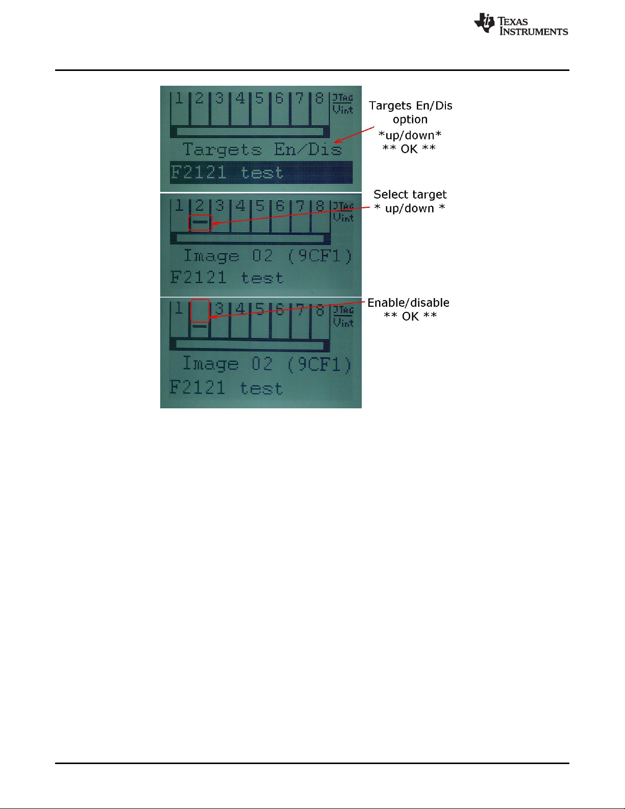
Figure 2-11. Target Enable or Disable Option
In addition to the these options that control programming, the contrast of the LCD display can be changed.
Select the Contrast option in the main menu, and press OK. Then use the up and down arrow buttons to
adjust the screen contrast. Changes to contrast reset after power down, unless the contrast setting has
been set by the GUI on the host computer.

www.ti.com
Programming MSP Flash Devices Using the MSP Gang Programmer
33
SLAU358Q–September 2011–Revised October 2019
Submit Documentation Feedback
Copyright © 2011–2019, Texas Instruments Incorporated
Operation
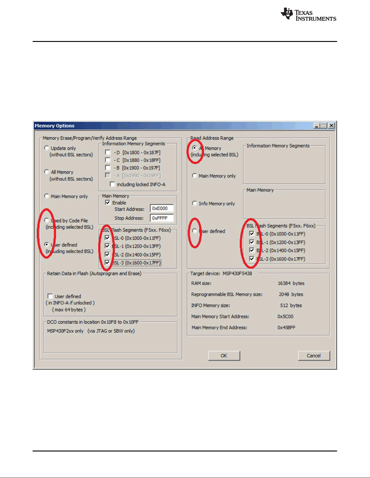
2.1.5 Memory Setup for GO, Erase, Program, Verify, and Read
The GO, Erase, Program, Verify, and Read operations shown in Figure 2-1 use addresses specified in the
Memory Options dialog screen shown in Figure 2-2. The memory setup used by these operations has five
main options:
1. Update only – When this option is selected, the GO operation does not erase memory contents.
Instead contents of code data taken from the code file are downloaded to flash memory. This option is
useful when a relatively small amount of data, such as calibration data, needs to be added to flash
memory. Other address ranges should not be included in the code file, meaning that the code file
should contain ONLY the data which is to be programmed to flash memory. For example, if the code
file contains data as shown in TI format:
@1008
25 CA 80 40 39 E3 F8 02
@2200
48 35 59 72 AC B8
q
Then 8 bytes of data are written starting at location 0x1008 and 6 bytes of data starting at location
0x2200. The specified addresses should be blank before writing (contain a value of 0xFF). Before the
writing operation is actually performed, the MSP Gang Programmer automatically verifies if this part of
memory is blank and proceeds to program the device only if verification is successful.
NOTE: Even Number of Bytes
The number of bytes in all data blocks must be even. Words (two bytes) are used for writing
and reading data. In case that the code file contains an odd number of bytes, the data
segment is appended by a single byte containing a blank value of 0xFF. This value does not
overwrite the current memory contents (because Update only is selected), but verification
fails if the target device does not contain a blank value of 0xFF at that location.
2. All Memory – This is the most frequently used option during programming. All memory is erased before
programming, and all contents from the code file are downloaded to the target microcontroller's flash
memory. When the microcontroller contains an INFO-A segment that can be locked (for example the
MSP430F2xx series contains DCO constants at locations 0x10F8 to 0x10FF), then INFO-A can be
erased or left unmodified. The including locked INFO-A segment should be selected or unselected
respectively. When INFO-A is not erased, none of the data is saved into INFO-A, even if this data is
specified in the code file. In addition, the DCO constants in the Retain Data in Flash group should be
selected if the DCO constants should be restored after erasing the INFO-A segment.
3. Main memory only – Flash information memory (segments A and B, C, D) are not modified. Contents
of information memory from the code file are ignored.
4. Used by Code File – This option allows main memory segments and information memory segments to
be modified when specified by the code file. Other flash memory segments are not touched. This
option is useful if only some data, like calibration data, needs to be replaced.
5. User defined – This option is functionally similar to options described before, but memory segments
are explicitly chosen by the user. When this option is selected, then on the right side of the memory
group, in the Memory Options dialog screen, check boxes and address edit lines are enabled. The
check boxes allow the user to select information memory segments to be enabled (erased,
programmed, verified). Edit lines in the Main Memory group allow the user to specify the main memory
address range (start and stop addresses). The start address should specify the first byte in the
segment, and the stop address should specify the last byte in the segment (last byte is programmed).
Because the main memory segment size is 0x200, the start address should be a multiple of 0x200; for
example, 0x2200. The stop address should specify the last byte of the segment to be written.
Therefore, it should be greater than the start address and point to a byte that immediately precedes a
memory segment boundary; for example, 0x23FF or 0x55FF.
Programming MSP Flash Devices Using the MSP Gang Programmer
www.ti.com
34
SLAU358Q–September 2011–Revised October 2019
Submit Documentation Feedback
Copyright © 2011–2019, Texas Instruments Incorporated
Operation
2.1.5.1 Writing and Reading BSL Flash Sectors in the MSP430F5xx and MSP430F6xx MCUs
The MSP430F5xx and MSP430F6xx microcontrollers have BSL firmware saved in flash memory sectors.
By default, access to these sectors (Read or Write) is blocked, however it is possible to modify the BSL
firmware if required, which allows the user to upload newer or custom defined BSL firmware. These BSL
sectors are located in memory starting at 0x1000 to 0x17FF. The MSP Gang Programmer software
handles modification of these BSL flash sectors using the same method as all other memory sectors.
However, to avoid unintentional erasing of BSL sectors, the most commonly used memory option, All
Memory , blocks access to these BSL sectors. Access to BSL sectors is unlocked only when the Used by
Code File or User defined option is selected and desired selected BSL sectors are enabled, as shown in
Figure 2-12. Contents of BSL sectors can be read even when the All Memory option is selected.
NOTE: The user can select which segments of memory are written to or read from. The selected configuration
shows how the user can configure the programmer to overwrite segments of memory used by the Bootloader
(BSL).
Figure 2-12. Memory Options, BSL Sectors Selected