SIPLACE S-23 HM - 第185页
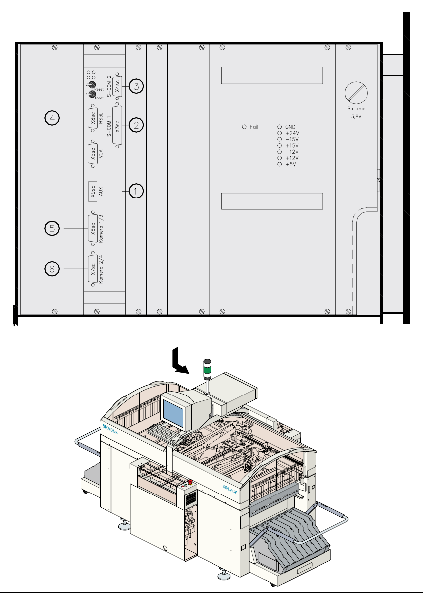
User Manual SIPLAC E S-23 HM 6 Vision functions Software Version SR.406.xx 02/00 US Edition 6.1 The vision systems on the placement system 185 Key to Fig. 6.1 - 4 (1) MVS 340 visi on ana lysis unit (2) COM1 interface (3)…
6 Vision functions User Manual SIPLACE S-23 HM
6.1 The vision systems on the placement system Software Version SR.406.xx 02/00 US Edition
184
6
Fig. 6.1 - 4 Vision analysis unit
User Manual SIPLACE S-23 HM 6 Vision functions
Software Version SR.406.xx 02/00 US Edition 6.1 The vision systems on the placement system
185
Key to Fig. 6.1 - 4
(1) MVS 340 vision analysis unit
(2) COM1 interface
(3) COM2 interface
(4) HS
3
L interface
(5) Camera connections:
1 PCB camera, gantry 1
3 Component camera, gantry 1
(6) Camera connections:
2 PCB camera, gantry 2
4 Component camera, gantry 2
6
The electronic image signals from components, PCB fiducials and feeder module fiducials can be
transferred from the vision analysis unit via the video multiplexer to the station monitor, where they
are used for measuring and testing purposes. 6
6 Vision functions User Manual SIPLACE S-23 HM
6.2 PCB vision system Software Version SR.406.xx 02/00 US Edition
186
6.2 PCB vision system
The PCB vision system records the precise position of the PCB by measuring fiducials, and cal-
culates the offset in the x and y directions, the angle of rotation relative to the PCB transport di-
rection and the shear acting on the PCB. Reject fiducials (ink spots) are also recorded and
analyzed by the PCB vision system. 6
6.2.1 System description
The PCB vision system for detecting the position of PCBs consists of the optical PCB position de-
tection system and the vision analysis unit. 6
Optical PCB position detection system 6
Each gantry has a separate PCB position detection system (see Fig. 6.1 - 3 on page 182). 6
Vision analysis unit 6
The control unit of each placement system contains one analysis unit for detecting the position of
PCBs and components (see Fig. 6.1 - 4 on page 184). 6
A CCD camera (SONY XC75) with integral mapping and illumination lens forms the optical PCB
position detection system. The field of view of the PCB module is 5.7 mm x 5.7 mm. The size and
position of the search field can be programmed as required within the fields of view. The mapping
lens is a special measuring lens which corrects most errors caused by the curvature of the PCB.
The illumination is switched on only while fiducials are being recorded. 6
The vision analysis unit (MVS) is a single-board system conforming to VME standards. The hard-
ware consists of 6
– the MVS motherboard with vision processor and interface connections
– and the MVS camera interface for up to four CCD cameras.
MVS motherboard with vision processor and interface connections 6
The two VME bus connections are located on the back of the VME module. 6
The front panel of the VME module contains connectors for 6
– the monitor (VGA mode, 15-pin SUBD connector)
– the high-speed interface (HS
3
L), 9-pin SUBD connector
– up to 4 camera inputs (2 x 15-pin SUBD connector)
– two serial interfaces (RS232 for COM1 with a 25-pin SUBD connector and COM2 with a
9-pin SUBD connector)