SPF维修.pdf - 第73页
SPF 4.4 Recognition Illumination Related Matter SERVICE MANUAL 4.4−2 D54SEC−W4−000−B0 5. Measure the brightness level when selecting the PCB RECOGNITION CAMERA for CAMERA and SPOT (white LED) for LIGHT TYPE on the ’RECOG…
4.4 Recognition Illumination Related Matter
SERVICE MANUAL
SPF
4.4−1
D54SEC−W4−000−B0
4.4 Recognition Illumination Related Matter
D54SEC−W4−000−B0
Sentence No.
4.4.1 PCB Recognition Camera Brightness Adjustment
Unit No.
PCB Recognition Camera
Brightness Adjustment
=Preparation=
1. Brightness adjustment jig
2. (−) driver (small)
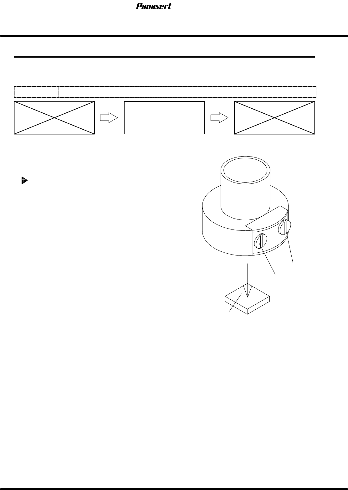
PCB recognition camera brightness
adjustment
=CHECK=
Since the brightness changes gradually, be
sure to check the brightness within 5 minutes
after illuminating the LED.
1. Place the brightness adjustment jig on the PCB.
2. Set the PCB on the transfer rail.
=HINT=
Be sure to fix the brightness adjustment jig
with the adhesive tape, etc.
3. Select PCB RECOGNITION CAMERA on the
’RECOGNITION SERVICE’ screen of the secret
screen and project the image of the PCB
recognition camera on the recognition monitor.
=REFERENCE=
Referto’RELATEDINFORMATION/Secret
ScreenServiceFunctions(CONFIDENTIAL)’
in this manual.
4. Raise the ST axis until the focus of the PCB
recognition camera focalizes on the brightness
adjustment jig and project the image of the
brightness adjustment jig.
VR2
(Ring)
VR1
(Spot)
Brightness adjustment jig
PCB recognition camera
SPF
4.4 Recognition Illumination Related Matter
SERVICE MANUAL
4.4−2
D54SEC−W4−000−B0
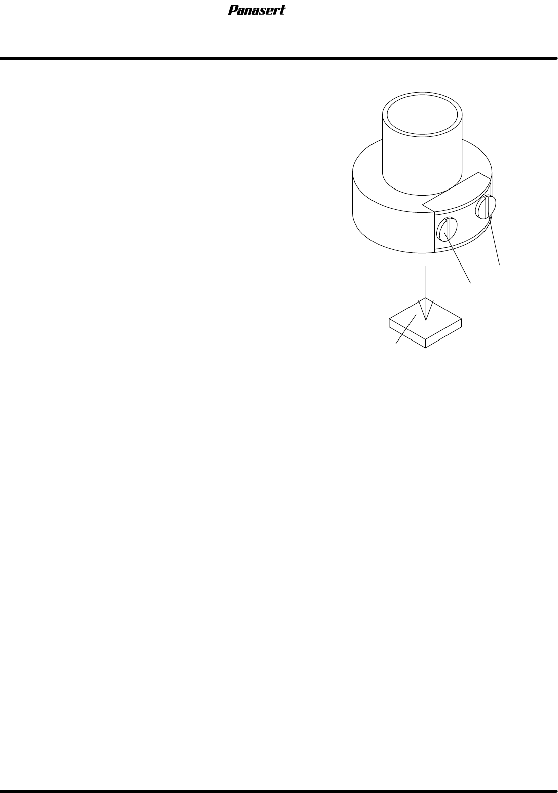
5. Measure the brightness level when selecting the
PCB RECOGNITION CAMERA for CAMERA and
SPOT (white LED) for LIGHT TYPE on the
’RECOGNITION SERVICE’ screen of the secret
screen.
=HINT=
Be sure to set the size of the brightness
density measurement window to 50mm as
the measured value on the monitor.
6. Turn “RECOG LIGHT SPOT” on the sub control
panel [ON].
7. Rotate the VR1 to adjust the brightness to 40.
=Specification=
Brightness level : 40 ± 4
8. Turn “RECOG LIGHT SPOT” on the sub control
panel [OFF] and “RECOG LIGHT RING” [ON].
9. Rotate the VR2 to adjust the brightness to 50.
=Specification=
Brightness level : 50 ± 5
VR2
(Ring)
VR1
(Spot)
Brightness adjustment jig
PCB recognition camera
4.4 Recognition Illumination Related Matter
SERVICE MANUAL
SPF
4.4−3
D54SEC−W4−000−B0
4.4.2 PCB Recognition Camera Focus Adjustment in
Screen Recognition
Unit No. 1080815100
PCB Recognition Camera Focus
Adjustment in Screen
Recognition
Maintenance Manual /
Maintenance Guide / PCB
Recognition Camera Focus and
Parallelism Adjustment
=Preparation=
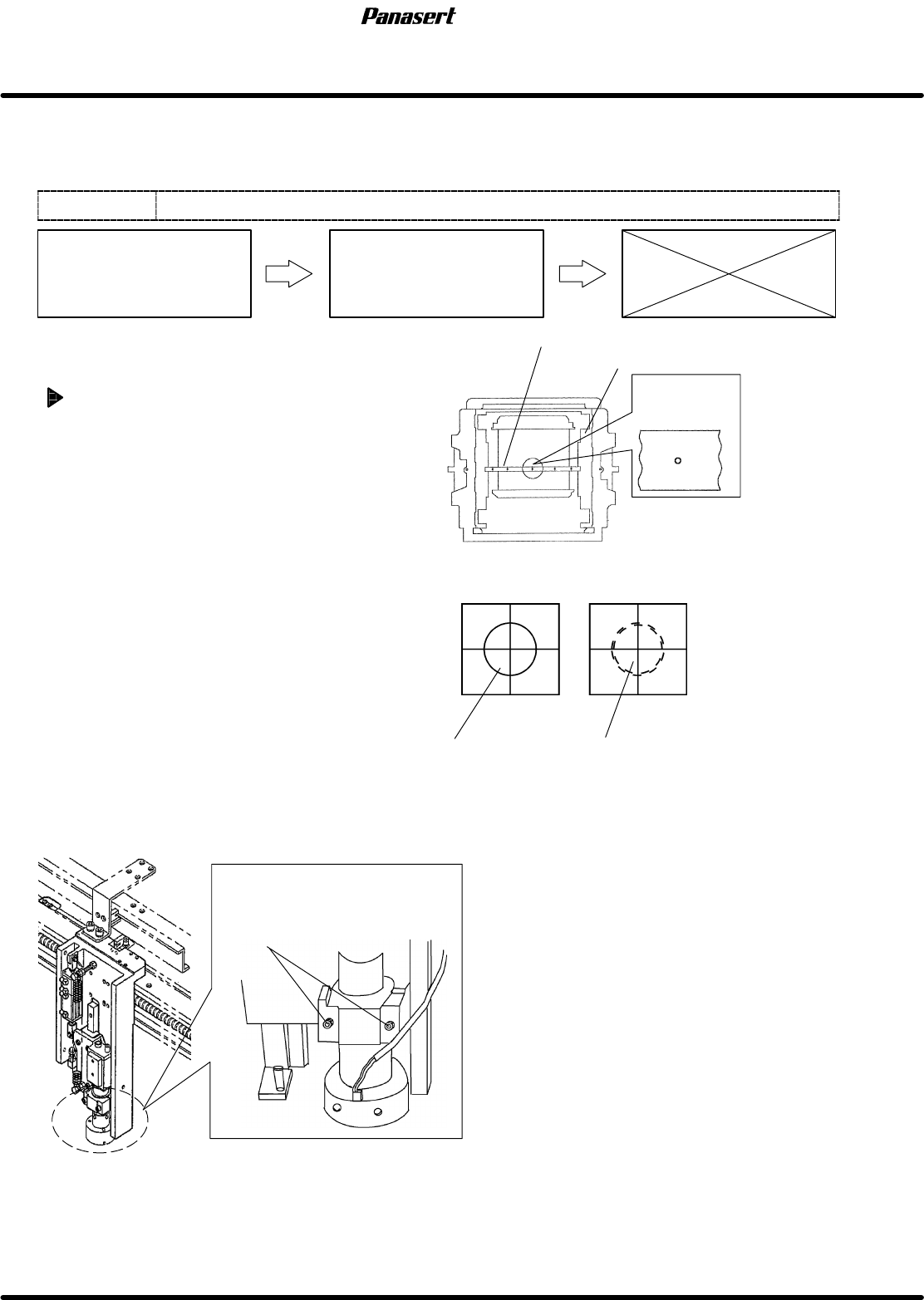
1. Mark plate jig
PCB recognition camera focus
adjustment in screen recognition
1. Turn the power [ON] and return to origin.
2. Fix the mark plate jig on the screen position
correction table with bolts (4 pcs.).
3. Move the PCB recognition camera to the
camera mark (the mark for center) on the
mark plate jig.
=CHECK=
Be sure to move the CY axis (camera Y
axis ) to −490mm and the CX axis
(camera X axis) to 0mm.
4. Turn “RECOG LIGHT RING” on the sub control
panel [ON].
5. Display the camera mark on the monitor
screen.
6. Adjust the camera height until the camera
focalizes to the camera mark.
=CHECK=
Be sure to loosen the PCB recognition
camera holder bolts to adjust.
Camera mark
OK
NG
Mark plate jig
Camera mark
is in focus.
Camera mark is out of focus.
Camera mark on the monitor screen
Screen position correction table
PCB recognition camera
holder bolts