2500_Users_Manual-.pdf - 第375页
V0001C01010101NHLLLHHLH LN* V0002C01011111NHLLHLLLH LN* V0003C10010111NZZZZZZZZ ZN* V0004C01010100NFLHHLFFL LN* Translation Formats The following example uses the V field to specify functional test information for a devi…
Translation
Formats
Test
Field
(V
field)
<
function
test>
::
=
[<pin
list〉]
<test
vector>
{<test
vector>}
<pin
number>
::
=
<
delimiter
>
<number>
N
::
=
number
of
pins
on
device
<test
vector>
::
=
'V'
<number>
<delimiter>
<
test
condition〉
:
N
vtest
condition〉
=
vdigit>
B
「CTDTFTHTKTLTN」P
|u「xtz,
〈
reserved
condition〉
::
=
'A'
|
E
|
'G'
|
T
|
'J'
|
'M'
|
'0'
|
Q
|
'R'
|
Functional
test
information
is
specified
by
test
vectors
containing
test
conditions
for
each
device
pin.
Each
test
vector
contains
n
test
conditions,
where
n
is
the
number
of
pins
on
the
device.
The
following
table
lists
the
conditions
that
can
be
specified
for
device
pins.
When
using
structured
test
vectors
to
check
your
logic
design,
do
NOT
use
101
or
010
transitions
as
tests
for
clock
pins:
use
C,
K,
U,
or
D
instead.
Test
Conditions
Drive
input
low
Drive
input
high
Drive
input
to
supervoltage
#2-9
Buried
register
preload
(not
supported)
Drive
input
low,
high,
low
Drive
input
low,
fast
slew
Float
input
or
output
Test
output
high
Drive
input
high,
low,
high
Verifies
that
the
specified
output
pin
is
low
Power
pins
and
outputs
not
tested
Preload
registers
Drive
input
high,
fast
slew
Output
not
tested,
input
default
level
Test
input
or
output
for
high
impedance
0
1
2-9
B
C
D
F
H
L
N
P
U
X
z
Note:
C,
K,
U,
and
D
are
clocking
functions
that
allow
for
setup
time.
The
C,
K,
U,
and
D
driving
signals
are
presented
after
the
other
inputs
are
stable.
The
L,
H,
and
Z
tests
are
performed
after
all
inputs
have
stabilized,
including
C,
K,
U,
and
D.
Test
vectors
are
numbered
by
following
the
V
character
with
a
number.
The
vectors
are
applied
in
numerical
order.
If
the
same
numbered
vector
is
specified
more
than
one
time,
the
data
in
the
last
vector
replace
any
data
contained
in
previous
vectors
with
that
number.
D-44
ProMaster
2500
User
Manual
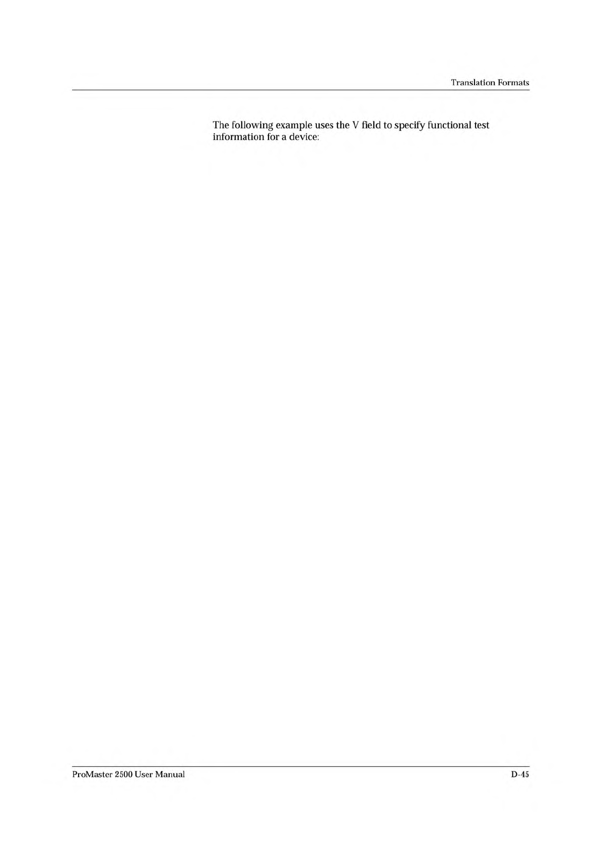
V0001C01010101NHLLLHHLHLN*
V0002C01011111NHLLHLLLHLN*
V0003C10010111NZZZZZZZZZN*
V0004C01010100NFLHHLFFLLN*
Translation
Formats
The
following
example
uses
the
V
field
to
specify
functional
test
information
for
a
device:
ProMaster
2500
User
Manual
D-45
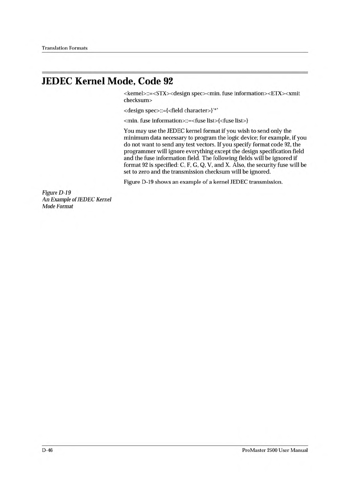
<STX>
Acme Logic Design Jane Engineer Feb. 29 1983
Widget Decode 756-AB-3456 Rev C Device Mullard 12AX7*
L0000 1111111011 1111111111 1111000000 0000000000
0000000000 0000000000 0000000000 0000000000
0000000000 0000000101 1111111111 1111111111
0000000000 0000000000 0000111101 1111111111
1111111111 1111110111 1111111111 1111111111*
L0200 1110101111 1111110000 0000000000 0000000000
1111111111 1111011011 1111111111 1111111110
0111111111 1111111111 1111111110 1111111111
1111111111 1111101111 1111111111 1111101111
0000000000 0000000000 0000*
<EXT>0000
0091-2
Translation
Formats
JEDEC
Kernel
Mode,
Code
92
<kernel>::=<STXxdesign
specxmin.
fuse
informationxETXxxmit
checksum〉
<design
spec>::={<field
character〉}'*'
<min.
fuse
information>::=<fuse
list>{<fuse
list〉}
You
may
use
the
JEDEC
kernel
format
if
you
wish
to
send
only
the
minimum
data
necessary
to
program
the
logic
device;
for
example,
if
you
do
not
want
to
send
any
test
vectors.
If
you
specify
format
code
92,
the
programmer
will
ignore
everything
except
the
design
specification
field
and
the
fuse
information
field.
The
following
fields
will
be
ignored
if
format
92
is
specified:
C,
F,
G,
Q,
V,
and
X.
Also,
the
security
fuse
will
be
set
to
zero
and
the
transmission
checksum
will
be
ignored.
Figure
D-19
shows
an
example
of
a
kernel
JEDEC
transmission.
Figure
D-
19
An
Example
of
JEDEC
Kernel
Mode
Format
D-46
ProMaster
2500
User
Manual