sh030106u.pdf - 第640页
APPENDIX App. - 9 App. 5.7.3 When us ing MR -J3- D05 with an MR- J4 seri es ser vo ampl if ier (1) System c onfigur ation diagr am The followi ng shows the connec tion tar gets of th e STO s witch an d STO releas e s wit…
APPENDIX
App. - 8
App. 5.7 Functions and configuration
App. 5.7.1 Summary
MR-J3-D05 has two systems in which the each system has SS1 function (delay time) and output of STO
function.
App. 5.7.2 Specifications
Safety logic unit model MR-J3-D05
Control circuit
power supply
Voltage 24 V DC
Permissible
voltage fluctuation
24 V DC ± 10%
Power supply
capacity
[A] 0.5 (Note 1, 2)
Compatible system 2 systems (A-axis, B-axis independent)
Shut-off input 2 points (duplex wiring) SDI
_
: (source/sink compatible) (Note 3)
Shut-off release input 1 point (duplex wiring) SRES
_
: (source/sink compatible) (Note 3)
Feedback input 1 point (duplex wiring) TOF
_
: (source compatible) (Note 3)
Input type Photocoupler insulation, 24 V DC (external supply), internal limited resistance 5.4 kΩ
Shut-off output
4 points (duplex wiring)
STO
_
: (source compatible) (Note 3)
SDO
_
: (source/sink compatible) (Note 3)
Output method
Photocoupler insulation, open-collector type
Permissible current: 40 mA/1 output, Inrush current: 100 mA/1 output
Delay time setting
A-axis: Select from 0 s, 1.4 s, 2.8 s, 5.6 s, 9.8 s, or 30.8 s.
B-axis: Select from 0 s, 1.4 s, 2.8 s, 9.8 s, or 30.8 s.
Accuracy: ±2%
Functional safety
STO, SS1 (IEC/EN 61800-5-2)
EMG STOP, EMG OFF IEC/EN 60204-1)
Safety
performance
Standard ISO 13849-1:2015 Category 3 PL d, EN IEC 62061, EN 61508 SIL2, IEC 61800-5-2
Response
performance (when
delay time is set to
0 s) (Note 4)
10 ms or less (STO input off → shut-off output off)
Mean time to
dangerous failure
(MTTFd)
MTTFd ≥ 100 [years] (516a)
Diagnosis
converge (DC avg)
DC = Medium, 93.1 [%]
Probability of
dangerous failures
per hour (PFH)
4.75 × 10
-9
[1/h]
Global
standards
CE marking
LVD: EN 61800-5-1
EMC: EN 61800-3
MD: EN ISO 13849-1:2015, EN 61800-5-2, EN IEC 62061
Structure Natural-cooling, open (IP rating: IP 00)
Environment
Ambient
temperature
0 °C to 55 °C (non-freezing), storage: -20 °C to 65 °C (non-freezing)
Ambient humidity 5 %RH to 90 %RH (non-condensing), storage: 5 %RH to 90 %RH (non-condensing)
Ambience Indoors (no direct sunlight), free from corrosive gas, flammable gas, oil mist, dust, and dirt
Altitude Max. 1000 m above sea level
Vibration
resistance
5.9 m/s
2
at 10 Hz to 55 Hz (directions of X, Y and Z axes)
Mass [kg] 0.2 (including CN9 and CN10 connectors)
Note 1. Inrush current of approximately 1.5 A flows instantaneously when turning the control circuit power supply on. Select an
appropriate capacity of power supply considering the inrush current.
2. Power-on duration of the safety logic unit is 100,000 times.
3.
_
: in signal name indicates a number or axis name.
4. For the test pulse input, contact your local sales office.
APPENDIX
App. - 9
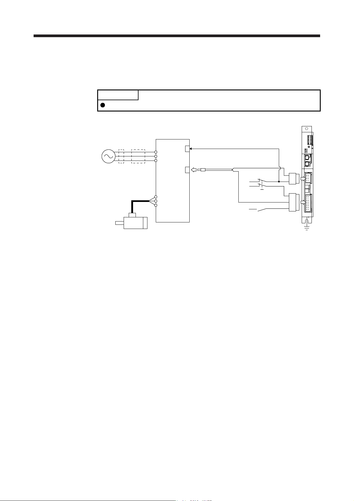
App. 5.7.3 When using MR-J3-D05 with an MR-J4 series servo amplifier
(1) System configuration diagram
The following shows the connection targets of the STO switch and STO release switch.
POINT
MR-D05UDL_M (STO cable) for MR-J3 series cannot be used.
MR-J3-D05
FG
STO switch
STO release switch
Magnetic
contactor
MCCB
Power
supply
Servo motor
MR-J4_B_(-RJ)
STO cable
MR-D05UDL3M-B
CN9
CN10
CN8
CN3
L1
L2
L3
U
V
W
EM2 (Forced stop 2)
APPENDIX
App. - 10
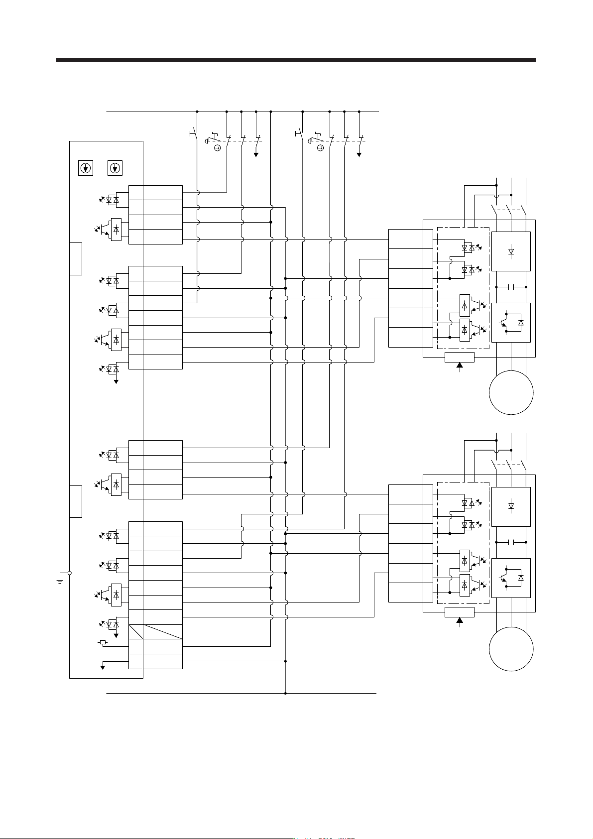
(2) Connection example
STO1
4
5
3
6
7
8
CN3
EM2 (B-axis)
CN8
SDO1A+4A
4B SDO1A-
SDI1A+1A
1B SDI1A-
SDI2A+
SRESA+
SDO2A+
TOFA
3A
3B
1A
1B
6A
6B
8A
SDI2A-
SDO2A-
SRESA-
CN9
CN10
STO1
TOFB2
TOFCOM
STO2
STOCOM
TOFB1
MR-J4_B_(-RJ)
FG
4
5
3
6
7
8
CN3
EM2 (A-axis)
CN8
TOFB2
TOFCOM
STO2
STOCOM
TOFB1
MR-J4_B_(-RJ)
SDO1B+3A
3B SDO1B-
SDI1B+2A
2B SDI1B-
SDI2B+
SRESB+
SDO2B+
TOFB
4A
4B
2A
2B
5A
5B
8B
+24V7A
0V7B
SDI2B-
SDO2B-
SRESB-
CN9
CN10
MR-J3-D05
S1
24 V
0 V
STOA
S3
STOB
MC
M
Servo motor
MC
M
Servo motor
Control circuit
Control circuit
CN8A
CN8B
EM2
(A-axis)
EM2
(B-axis)
SW1 SW2
(Note 1) (Note 1)
(Note 2) (Note 2)
RESA RESB
S4
S2
Note 1. Set the delay time of STO output with SW1 and SW2. These switches are located in a recessed area to prevent accidental
settin
g
chan
g
es.
2. To release the STO state
(
base circuit shut-off
)
, turn RESA and RESB on and turn them off.