KY8030 Programmers Manual - 第56页
54 | KY-8030 Series (KYOS-2007001_rev0) 3D In ‐ line Solder Paste Inspection Systems 1.3.5. V iew 1) Position Display the position of the sel ected flash, trace or pa d as an offse t distance f rom the specif…
Programmers Manual
| 53
Clearance
The clearance range required for the "Create All Patterns" and "Scan
Reference" tasks.
All positions within the clearance range are recognized as the same
position.
※ Note: If the PCB unit is mm, clearance 1 ==> 0.0001 mm.
If the PCB unit is inches, clearance 1 ==> 0.0001 inch.
Exclude flash
Indicates whether a flash will be excluded during create all pattern
process.
Exclude trace
Indicates whether a trace will be excluded during create all pattern
process.
Exclude multi-
pads pattern
Indicates whether adjacent pads will be differentiated during create all
pattern process.
You can prevent adjacent pads from being automatically registered as
a single pattern while performing "Create All Patterns".
Exclude nonbase
pads
Indicates whether flashes and traces in a layer will be excluded during create all
pattern process.
Remove current
pads
Indicates whether all patterns and pads registered will be removed
during create all pattern process.
Check duplicated
codes
Indicates whether duplication of part reference codes will be checked
and whether a warning message will be displayed.
Default
Initialize all settings back to the default settings set at the time of
shipment.
Ú Caution: If an option setting is changed, "Create All Patterns" may not be performed properly.
Ú Note: You can select from the following options for "Create All Patterns":
y Exclude flash
y Exclude trace
y Exclude multi-pads pattern
y Create All Patterns
y Exclude Nonbase pads
y Remove current pads
Ú Note: You can select the following option for "Scan Reference":
y Check duplicated codes
54 | KY-8030 Series(KYOS-2007001_rev0)
3DIn‐lineSolderPasteInspectionSystems
1.3.5. View
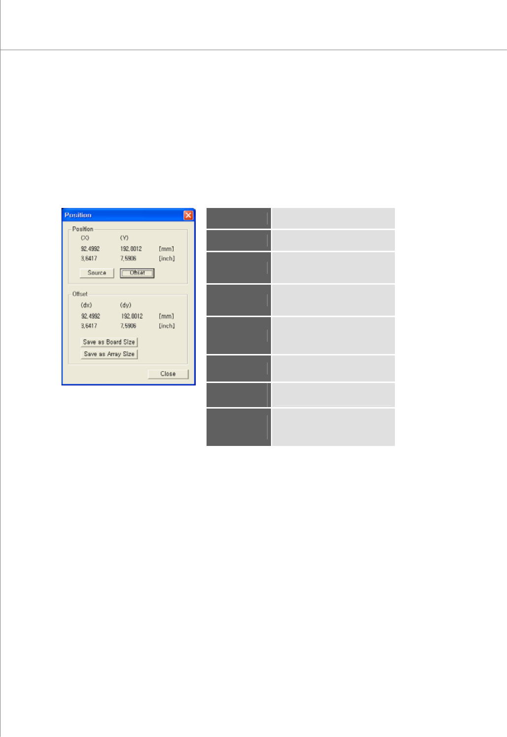
1) Position
Display the position of the selected flash, trace or pad as an offset distance from the
specified reference point.
You can specify PCB and array sizes directly.
The "Position" Dialog Box
Position (X)
The center for the selected point
in the X-axis
Position (Y)
The center for the selected point
in the Y-axis
Offset (dx)
The offset distance between the
selected point and the reference
point (source) in the X-axis
Offset (dy)
The offset distance between the
selected point and the reference
point (source) in the Y-axis
Source
Specify the current point as a
reference point.
Initial Value = (0,0)
Offset
Calculate and display offset (dx)
and offset (dy).
Save as Board
Size
Save offset (dx) and offset (dy)
values as a PCB size.
Save as Array
Size
Save offset (dx) and offset (dy)
values as the row and column
sizes for an array board.
Programmers Manual
| 55
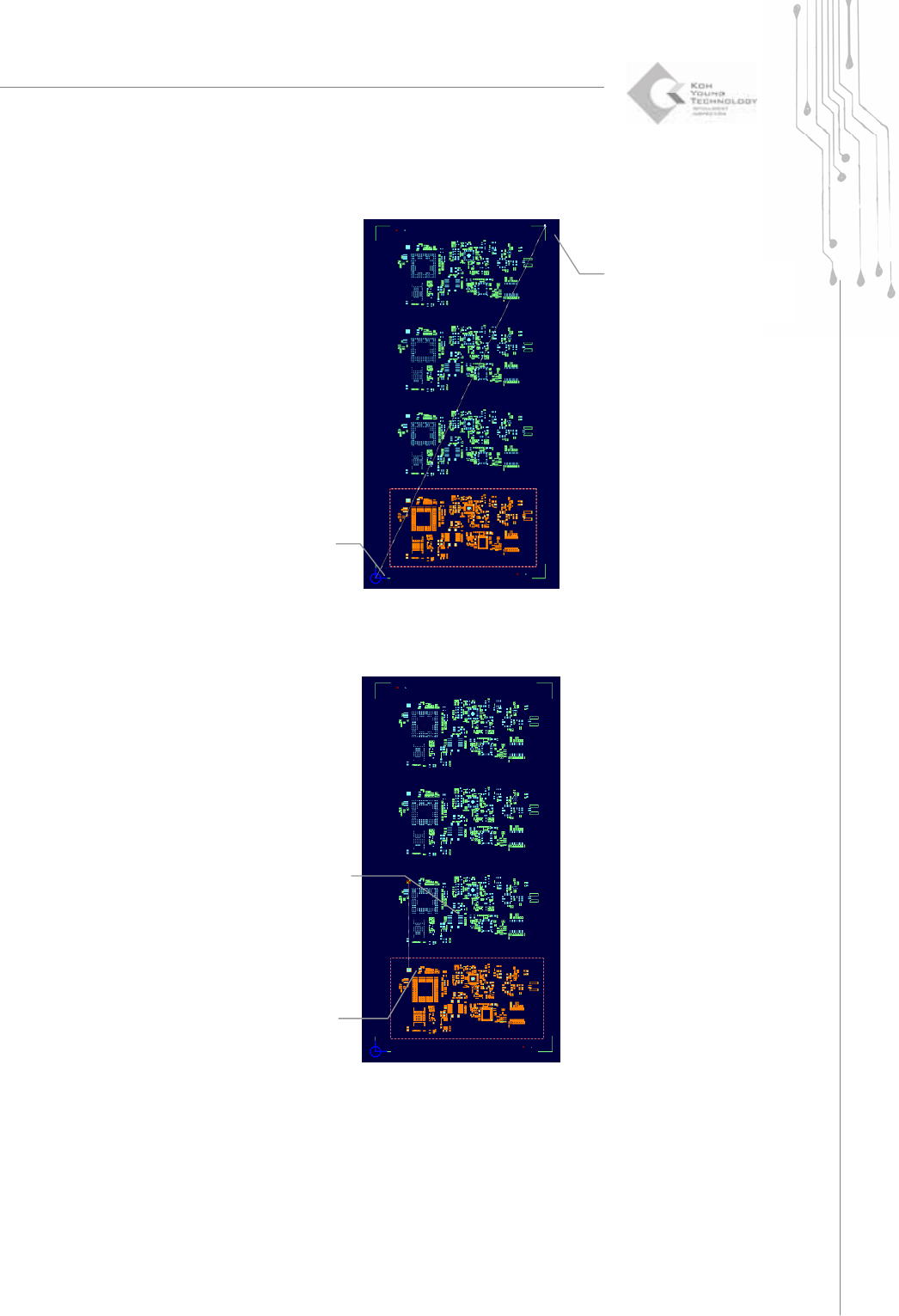
Ú Resizing a PCB
Ú Specifying the spacing of an array board
(1) Select Source
position
(2) Offset calculating
(1) Select Source
position
(2)Offset calculating