KY8030 Programmers Manual - 第75页
Programmers Manual | 73 3) Coplanarity Check un iformit y of the pad he ights in a co mponen t. ① With your mou se, specif y the area f or which you wa nt to ch eck coplan arity . ② After selec ting Copl anarit y , ent e…
72 | KY-8030 Series(KYOS-2007001_rev0)
3DIn‐lineSolderPasteInspectionSystems
7)
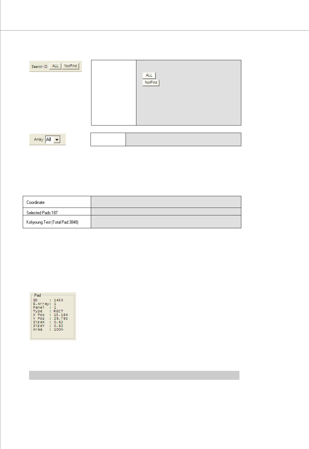
Search ID
Compare a pad file with a CAD file to find any
inconsistency.
* ALL: Check all pads.
* NotFind:
Check pads that do not match the CAD.
The All button works via the component ID
frame interface in 5.1.7 4). After modifying
the component ID, make sure to press the All
button to apply changes.
8)
Array
When using an array board, select all arrays or a
certain array number.
2.1.6. Status Bar
The status bar at the bottom of the screen shows the number of pads, positions of pads
and the file name.
Coordinate: Shows a variety of information on the selected pad.
Selected Pads: Shows the number of pads.
File Name & Total Pads : Shows a file name and the number of
pads.
2.1.7. Left Job Panel
1) Pad
Display information on the selected pad.
Pad Information: ID, board array, panel, Component ID, type, X-position, Y-position,
size X, size Y and area.
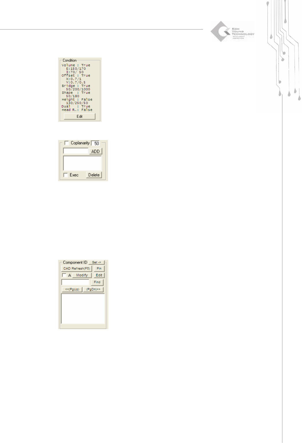
2) Inspection Conditions
Display inspection conditions for a pad.
You can edit these conditions by clicking the Edit button.
※ Note: For more information on specifying inspection conditions, see “6.3.3 6) Edit Job File”.
Programmers Manual
| 73
3) Coplanarity
Check uniformity of the pad heights in a component.
① With your mouse, specify the area for which you want to check coplanarity.
② After selecting Coplanarity, enter the upper/lower limits for the difference in heights.
③ Enter a name and click the ADD button. A new item will be registered in the following list
box.
④ Select Exec to perform inspection for the corresponding group.
4) Component ID
Display a component ID.
You can modify/edit/search for a Component ID by clicking the Modify/Edit/Find
button, respectively.
① Click the Pin button to display the pin number for the corresponding component.
② Click the CAD Refresh button to display the Component ID and contour lines.
③ Click the Modify button to move the CAD location of the selected component or to
adjust the order in which pin numbers are assigned.
④ Click the Edit button to change the settings for the library linked with the
corresponding component.
74 | KY-8030 Series(KYOS-2007001_rev0)
3DIn‐lineSolderPasteInspectionSystems
⑤ Click the SetÆbutton to set all component attributes for an array-type PCB to the current values.
2.2. Usage Example (Creating a Job File)
Basic procedure is like followings.
- Load Pad File.
- Input the thickness of the stencil mask.
- Set the Fiducials.
- Set the inspection condition for the pads.
- Import CAD file or Pin CAD file(When available).
- Save Job file. (*.mdb)
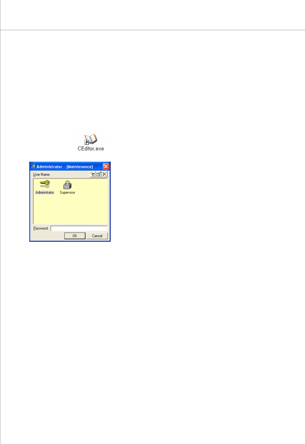
1) Double-click the
icon. A window will appear allowing you to select a
user account.
2) Select the desired user account, enter a password and click the OK button.
The CEditor program will be launched.
3) Click "File ▶ Load Pad file “ in the menu bar. The file selection window will appear.
4) Select a pad file (*.pad) and click the Open button. The selected file will be opened.
5) The following PCB setting window pops up.