KY8030 Programmers Manual - 第84页
82 | KY-8030 Series (KYOS-2007001_rev0) 3D In ‐ line Solder Paste Inspection Systems 4) Click the Set button. The duplicated CAD file data w ill be displayed. 5) Click the CAD Ref resh button or press t he F5…
Programmers Manual
| 81
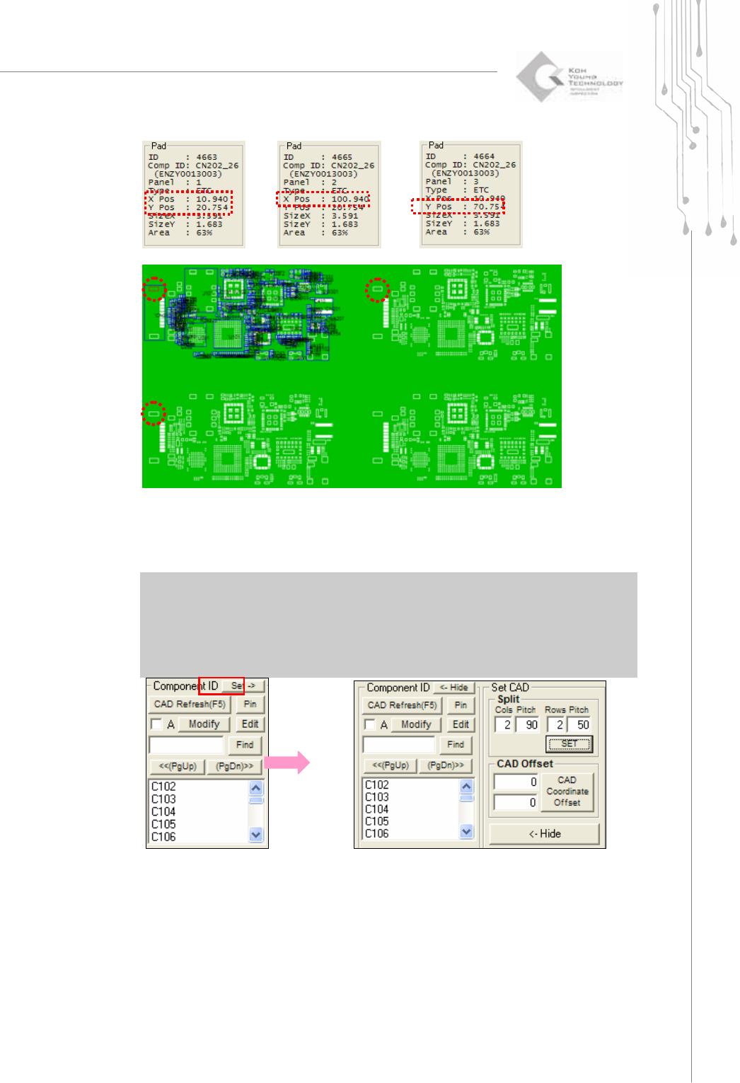
3) Click the Set button under the “Component ID”.
Because the board has two columns and two rows, enter 2 for Cols and 2 for Rows.
Pitch represents the spacing in the board. Enter 90 for Cols Pitch and 50 for Rows Pitch.
※ Note:
Cols Pitch = The X coordinate of the reference point for Board 2 - The X coordinate
of the reference point for Board 1.
Rows Pitch = The Y coordinate of the reference point for Board 3 - The Y coordinate
of the reference point for Board 1.
1
2
3
82 | KY-8030 Series(KYOS-2007001_rev0)
3DIn‐lineSolderPasteInspectionSystems
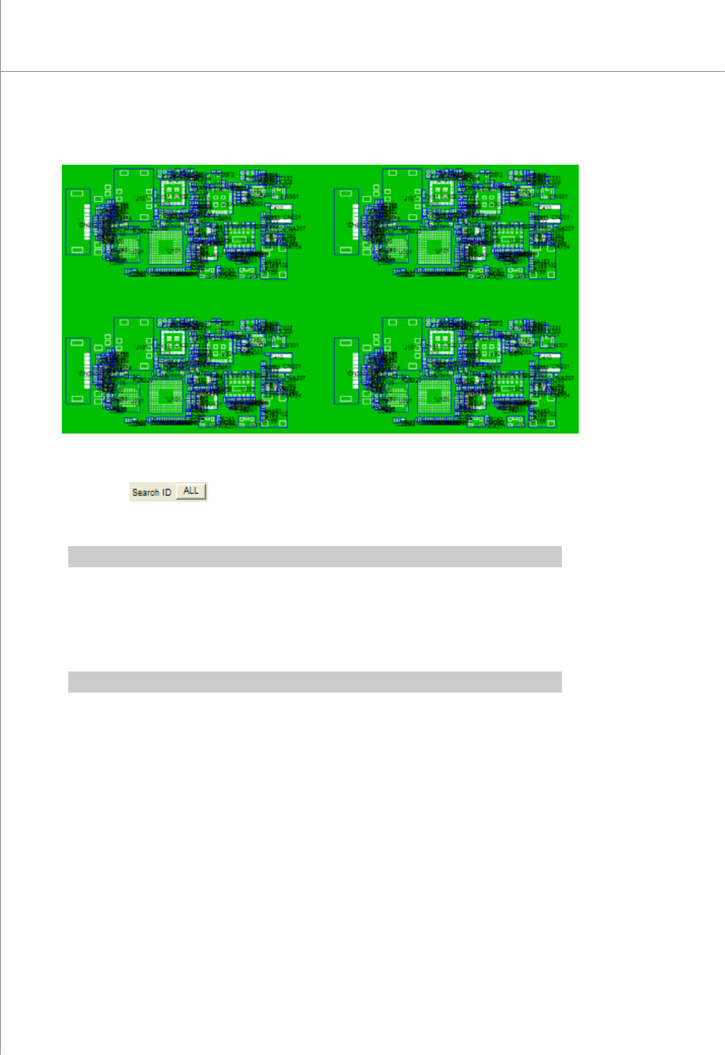
4) Click the Set button. The duplicated CAD file data will be displayed.
5) Click the CAD Refresh button or press the F5 key in the keyboard to display all
component and pin numbers.
6) Click the
button under the “Search ID”. Assign a pin number to the
matched pin CAD and pad data and register it. Save the registered pin number in a
job file.
※ Note: Click the Not Find button under the "Search ID" to display unmatched data.
7) Component ID for 2,3 and 4 array will be properly registered.
8) Click the Save button to save the job data in a job file.
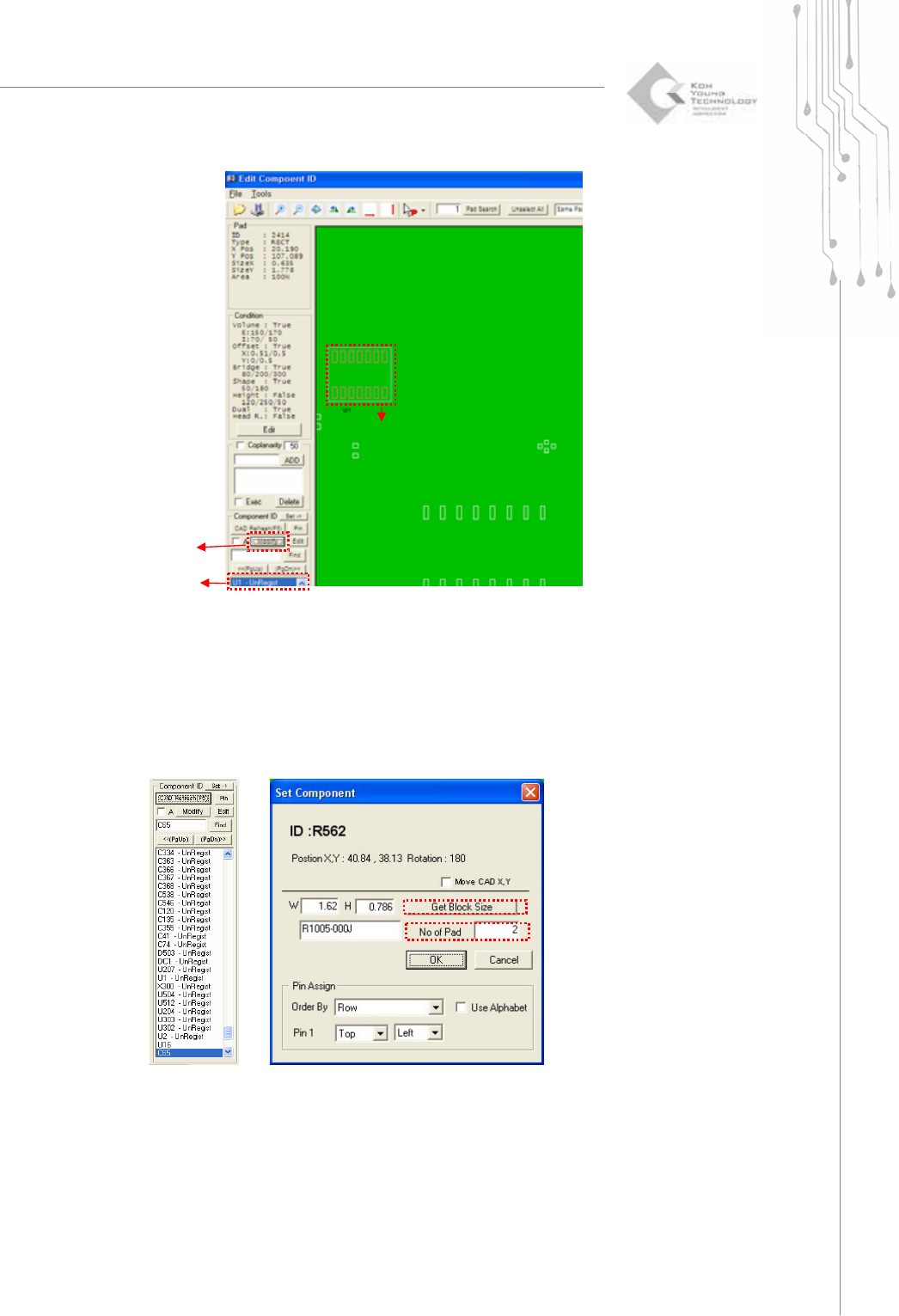
2.2.3. Modifying a Component ID
※ Note: Not applicable when pin CAD file is used..
1) Follow steps 1) - 11) in the previous example under 5.2.1.
Programmers Manual
| 83
2) Choose a not-matched component or component to be modified under the
“Component ID”.
3) Draw a box for that component ID in PCB display.
4) Click the Modify button.
The “Set Component” window will appear. Click OK.
②
①
③