Specification-SIPLACE-S25HM-eng - 第28页
26 Description In the cluster technology each subpanel is assigned an ink spot. If this is pres ent during the meas- urement via the PCB vision mod- ule, the corresponding subpanel is populated. It is also possible to ac…
25
Description
Different reference mark shapes
prove to be optimal depending on
the condition of the surface.
Particularly advisable for bare cop-
per surfaces with little oxidation is
the single cross. Maximum recog-
nition reliability is achieved due to
the high information content. Rec-
tangle, square and circle are less
”informative” but save space, are
rugged, and can even be used
when oxidation is at an advanced
stage.
Advisable for tinned structures are
circle or square because in this
case the ratio of the mark dimen-
sions to the presolder thickness is
particularly favorable.
Vision Sensor Technology:
PCB Position Recognition
Reference Mark Criteria
Locate 2 marks
Locate 3 marks in addition
X-/Y-position, rotation angle, mean distortion
Shear, distortion in X- and Y-direction
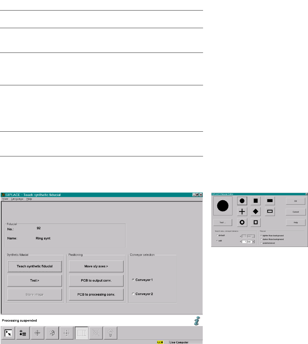
Mark shapes Synthetic marks e.g., circle, cross, square,
rectangle, rhombus, circular ring, square
ring, octagonal ring (choose from menu)
Mark surface:
Copper
Tin
Without oxidation and solder resist
Warp
≤ 1/10 of structure width,
both with good contrast to environment
Mark dimensions
Circle
Cross
Rectangle/square
Rhombus
Diameter: 0.3 - 3 mm
Length and width: 0.3 - 3 mm
Line thickness: 0.1 - 1.5 mm
Edge length: 0.3 - 3 mm
Transversal length:0.3 - 3 mm
Mark environment Clearance around reference mark not
necessary if there is no similar mark
structure in the search area
Teach Synthetic Fiducial
Fiducial Editor

26
Description
In the cluster technology each
subpanel is assigned an ink spot.
If this is present during the meas-
urement via the PCB vision mod-
ule, the corresponding subpanel is
populated. It is also possible to ac-
complish the population of the
subpanel when the ink spot is
missing. With this function it is
possible to eliminate costs due to
unnecessary population of faulty
subpanels.
Global Ink Spot
Global Ink SpotGlobal Ink Spot
Global Ink Spot
Each bad board evaluation needs
time, so naturally the consumed
time increases with the number of
subpanels per PCB. Using a global
ink spot can result in a significant
reduction of these secondary
times.
The PCB vision module searches
at positions taught before for the
defined fiducial. In case of recogni-
tion there is no following evalua-
tion of subpanels. The system al-
lows the customer to choose also
the opposite interpretation.
Position Recognition of Feeder
Position Recognition of FeederPosition Recognition of Feeder
Position Recognition of Feeder
The pick-up position of the com-
ponents can be determined pre-
cisely with the aid of the position
recognition of the feeder. It is acti-
vated each time after a change of
feeder or component table. The
offset in position relative to the
stored ideal position is determined
on the basis of fiducials on the
feeder modules using the PCB vi-
sion module. This provides a very
high pick-up reliability even for the
very first component. This is par-
ticularly important with small com-
ponents.
Vision Sensor Technology:
Bad Board Recognition
Position Recognition of Feeder
Ink Spot Criteria
Evaluationmethod
for fiducials
for structures
brightness method
contrast method
Shapes and sizes of
fiducials/structures for
brightness method
contrast method
square or circular forms
edge length/diameter 0.3 - 5 mm
rectangular forms
edge length 0.3 - 5 mm
Masking material mat dark (light-absorbing)
not recommended: white or shiny
Ink spot recognition time 0.3 s for each method

27
Description
The component vision modules
perform a critical contribution to
placement accuracy and reliability.
It dependably recognizes all pack-
age forms (= geometric dimen-
sions of the component) illumi-
nated at various angles from a
number of planes. To illuminate
each component optimally, the
luminosity of the individual planes
can be adjusted individually in 256
levels.
Aside from the dimension of the
SMD component, the vision sys-
tem determines the lead number
and pitch (lateral IC lead bend) as
well as the rotation angle and X-/Y-
offset. Components which are not
suitable are rejected and automati-
cally corrected in a repair cycle.
Rotational and X-/Y-offsets are cor-
rected at the turning station of the
Collect & Place Head or via the
gantry axes. A relevant X-/Y-pick-
up offset is calculated from the
positions of a number of compo-
nents from one track. This is fac-
tored in accordance with the self-
learning principle during the sub-
sequent pick-up of components.
Prior to placement the required
geometrical dimensions of one
component type are entered into
the package form (GF) editor, cre-
ating a synthetic model of the
SMD module. This task is simpli-
fied by the comprehensive on-line
information and Help system.
Later the central SIPLACE vision
system, to which all other vision
modules are connected, analyzes
the gray-scale picture of the com-
ponent vision module. To this end,
suitable algorithms are used for
the pertinent package type. Due to
the combination of algorithms, the
vision system also functions relia-
bly under the most difficult condi-
tions, e.g., in the case of different
reflection behavior by the leads or
disruptive influences from the out-
side.
The algorithms are used for all
component vision modules.
Vision Sensor Technology:
Algorithms to determine the X-/Y-Position and the
Rotation Angle of Components
Algorithm Component Determined on the basis of
Size Driven Chip the component’s outline
(profile/gradients)
Row Driven IC several component leads
(correlation method)
Corner Driven IC all component leads
(correlation method)
Lead Driven Complex IC each component connection
(High-Accuracy-Lead-Extraction method)
Grid/Ball/Bump BGA, µBGA,
Flip Chip
all defined balls and bumps
(gradients/ball or bump centering)