(TI)对半导体器件的长期存储评估.pdf - 第9页
Figure 10-10. Reflow Oven Figure 10-1 1. Substrate on T ransport Belt Figure 10-12. Ultrasonic Flux Cleaning Samples from T able 5-1 were tested for solderability with a typical sample size of 9-10 units per lot. Example…
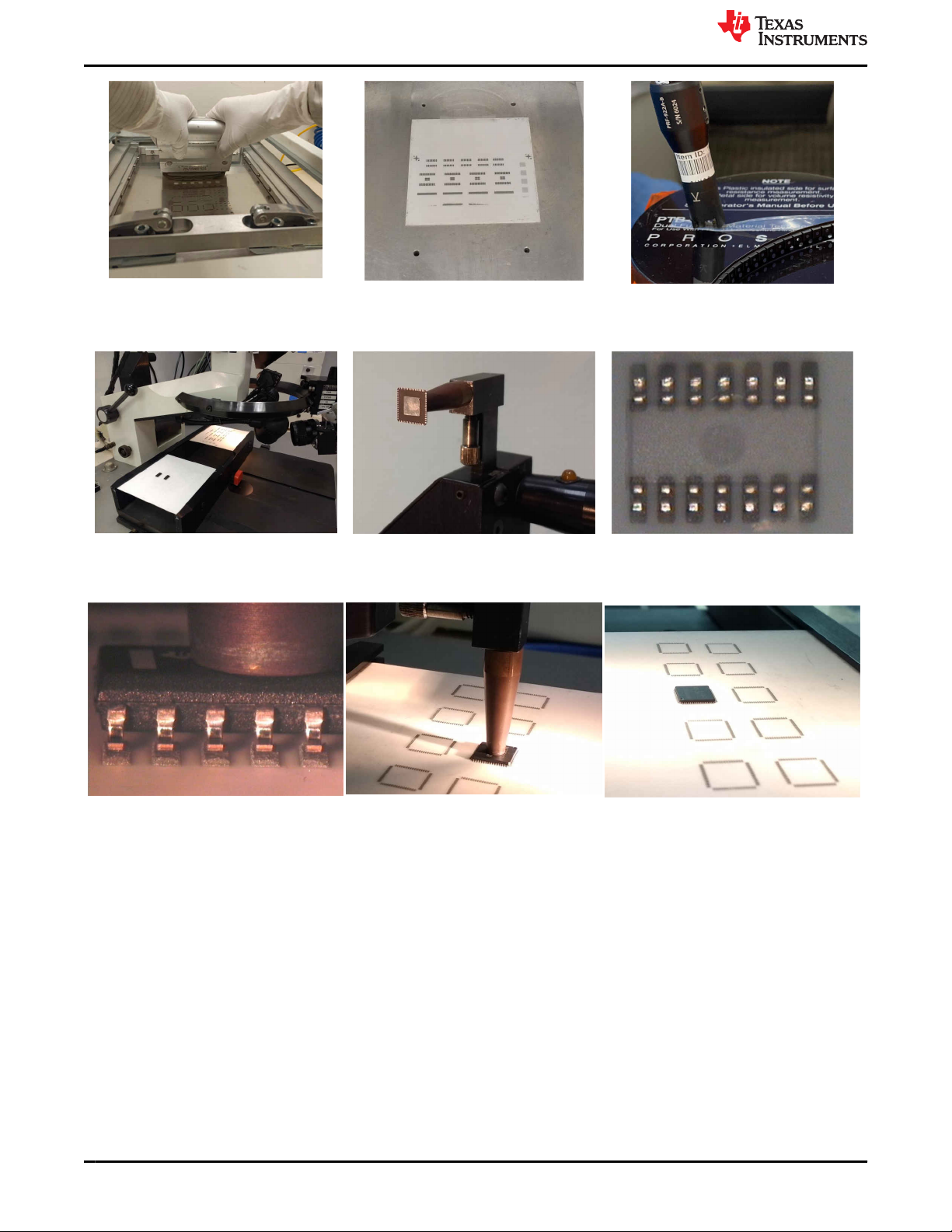
Figure 10-1. Solder Stencil in
Holder with Solder
Figure 10-2. Solder Paste Printed
Figure 10-3. Component
Placement Equipment
Figure 10-4. Component
Placement Equipment
Figure 10-5. Component
Placement Arm
Figure 10-6. Overlay Image
Package of Lead and Solder Paste
Figure 10-7. Side Camera View for
Final Placement Height
Figure 10-8. Placement Tool on
Substrate
Figure 10-9. Placed Component
on Substrate
The ceramic substrates were run through the convection reflow oven with a measured package temperature of
≈240°C and air atmosphere (Compressed Dry Air purge).
After reflow, the soldered products were cleaned in an ultrasonic bath with flux removal agent followed by DI
water rinse before the optical inspection of the solder wetting on the package leads.
Solderability Evaluation www.ti.com
8 Long Term Storage Evaluation of Semiconductor Devices SLPA019 – SEPTEMBER 2021
Submit Document Feedback
Copyright © 2021 Texas Instruments Incorporated
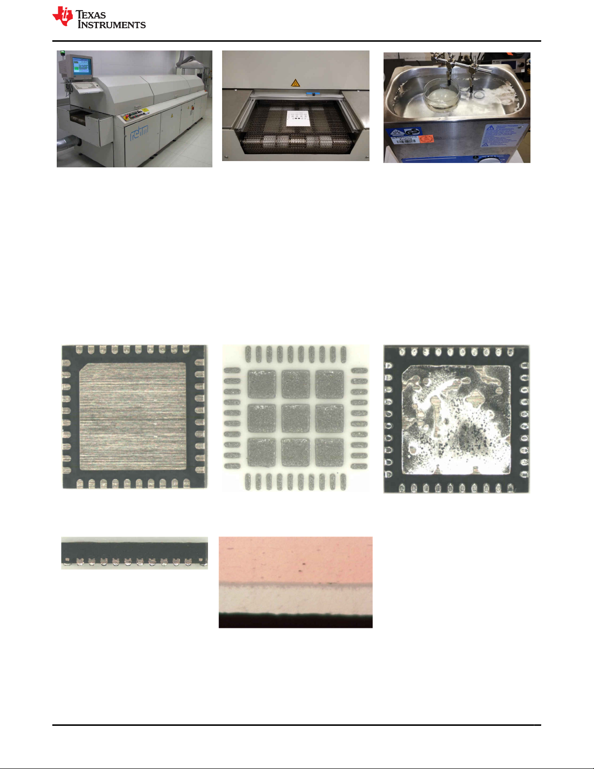
Figure 10-10. Reflow Oven
Figure 10-11. Substrate on
Transport Belt
Figure 10-12. Ultrasonic Flux
Cleaning
Samples from Table 5-1 were tested for solderability with a typical sample size of 9-10 units per lot. Example
images from the different packages and storage time are shown in the Section 11.1.
The package samples used for solderability testing were picked out of the tape and reel or from tubes baked for
four hours at 155°C in dry air to simulate standard J-STD-002 aging and then placed on the printed solder paste
pattern on the ceramic plate.
11 Solderability Test Results
11.1 Leadless Package
Sample batch #6: 13 years storage, MSL 3, lead finish: NiPdAu
Figure 11-1. Unit After Bake 4Hr/
150°C
Figure 11-2. Solder Paste Print
Patern
Figure 11-3. Bottom View After
Test
Figure 11-4. Side View
Figure 11-5. Cross Section
Through Thermal Pad, Showing
Intermatillic Between Base Ni
Layer on Copper and Solder
www.ti.com Solderability Test Results
SLPA019 – SEPTEMBER 2021
Submit Document Feedback
Long Term Storage Evaluation of Semiconductor Devices 9
Copyright © 2021 Texas Instruments Incorporated
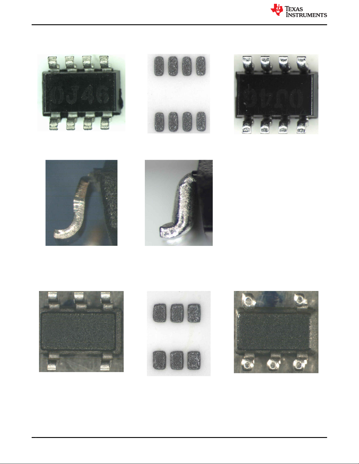
11.2 SOT (Small Outline Transistor) Package
Sample batch #30: 11 years storage, MSL2, SOT23 DCN, lead finish: post assembly Tin (Sn) plated
Figure 11-6. Unit After Bake 4hr/
150°C
Figure 11-7. Print Pattern
Figure 11-8. Bottom View After
Test
Figure 11-9. Lead Side View After
Bake
Figure 11-10. Lead Side View After
Soldering
Sample batch #21: 17 years storage, MSL1, SOT23 DBV, lead finish: pre-plated NiPdAu
Figure 11-11. Unit After Bake 4hr/
150°C
Figure 11-12. Print Pattern
Figure 11-13. Bottom View After
Test
Solderability Test Results www.ti.com
10 Long Term Storage Evaluation of Semiconductor Devices SLPA019 – SEPTEMBER 2021
Submit Document Feedback
Copyright © 2021 Texas Instruments Incorporated