Specification SIPLACE CS-Speed - 第19页
17 Description In the cluster technology each subpanel is assigned an ink spot. If this is pres ent during the meas- urement via the PCB vision mod- ule, the corresponding subpanel is populated. It is also possible to ac…
16
Description
Different reference mark shapes
prove to be optimal depending on
the condition of the surface.
Particularly advisable for bare cop-
per surfaces with little oxidation is
the single cross. Maximum recog-
nition reliability is achieved due to
the high information content. Rec-
tangle, square and circle are less
“informative” but save space, are
rugged, and can even be used
when oxidation is at an advanced
stage.
Advisable for tinned structures are
circle or square because in this
case the ratio of the mark dimen-
sions to the presolder thickness is
particularly favorable.
Vision Sensor Technology:
PCB Position Recognition
Reference Mark Criteria
Locate 2 marks
Locate 3 marks in addition
X-/Y-position, rotation angle, mean distortion
Shear, distortion in X- and Y-direction
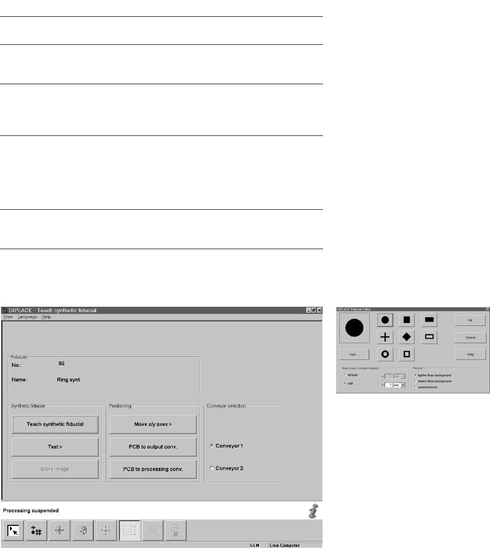
Mark shapes Synthetic marks e.g., circle, cross, square,
rectangle, rhombus, circular ring, square
ring, octagonal ring (choose from menu)
Mark surface:
Copper
Tin
Without oxidation and solder resist
Warp
≤ 1/10 of structure width,
both with good contrast to environment
Mark dimensions
Circle
Cross
Rectangle/square
Rhombus
Diameter: 0.3 - 3 mm
Length and width: 0.3 - 3 mm
Line thickness: 0.1 - 1.5 mm
Edge length: 0.3 - 3 mm
Transversal length: 0.3 - 3 mm
Mark environment Clearance around reference mark not
necessary if there is no similar mark
structure in the search area
Teach Synthetic Fiducial
Fiducial Editor

17
Description
In the cluster technology each
subpanel is assigned an ink spot.
If this is present during the meas-
urement via the PCB vision mod-
ule, the corresponding subpanel is
populated. It is also possible to ac-
complish the population of the
subpanel when the ink spot is
missing. With this function it is
possible to eliminate costs due to
unnecessary population of faulty
subpanels.
Global Ink Spot
Global Ink SpotGlobal Ink Spot
Global Ink Spot
Each bad board evaluation needs
time, so naturally the consumed
time increases with the number of
subpanels per PCB. Using a global
ink spot can result in a significant
reduction of these secondary
times.
The PCB vision module searches
at positions taught before for the
defined fiducial. In case of recogni-
tion there is no following evalua-
tion of subpanels. The system al-
lows the customer to choose also
the opposite interpretation.
Position Recognition of Feeder
Position Recognition of FeederPosition Recognition of Feeder
Position Recognition of Feeder
The pick-up position of the com-
ponents can be determined pre-
cisely with the aid of the position
recognition of the feeder. It is acti-
vated each time after a change of
feeder or component table. The
offset in position relative to the
stored ideal position is determined
on the basis of fiducials on the
feeder modules using the PCB vi-
sion module. This provides a very
high pick-up reliability even for the
very first component. This is par-
ticularly important with small com-
ponents.
Vision Sensor Technology:
Bad Board Recognition
Position Recognition of Feeder
Ink Spot Criteria
Evaluation method
for fiducials
for structures
brightness method
contrast method
Shapes and sizes of
fiducials/structures for
brightness method
contrast method
square or circular forms
edge length/diameter 0.3 - 5 mm
rectangular forms
edge length 0.3 - 5 mm
Masking material mat dark (light-absorbing)
not recommended: white or shiny
Ink spot recognition time 0.3 s for each method

18
Description
The standard component vision
module is directly integrated into
the Collect & Place Head. While
the component is cycling into the
next station of the Collect & Place
Head, the recorded image is eva-
luated by the central vision sys-
tem. The component rotation is
then corrected by the appropriate
angle based on the position off-
sets determined with vision in-
spection.
Vision Sensor Technology:
Standard Component Vision Modules for the 6-Nozzle
Collect & Place Head
Standard Component Vision Module for the 6-Nozzle C & P Head
Component size
minimum
maximum
0.6 x 0.3 mm
2
(0201)
18.7 x 18.7 mm
2
Component range See table on page 6
Camera’s field of view 24 x 24 mm
2
Illumination Front light
(3 freely programmable planes)
Pixel size 50 µm