IPC-SM-782A 表面安装设计和焊盘设计标准(带BGA).pdf - 第111页
1.0 SCOPE This subsection provides the component and land pattern dimensions for TO 252 (small outline transistor) components. Basic construction of the TO 252 device is also covered. At the end of this subsection is a l…
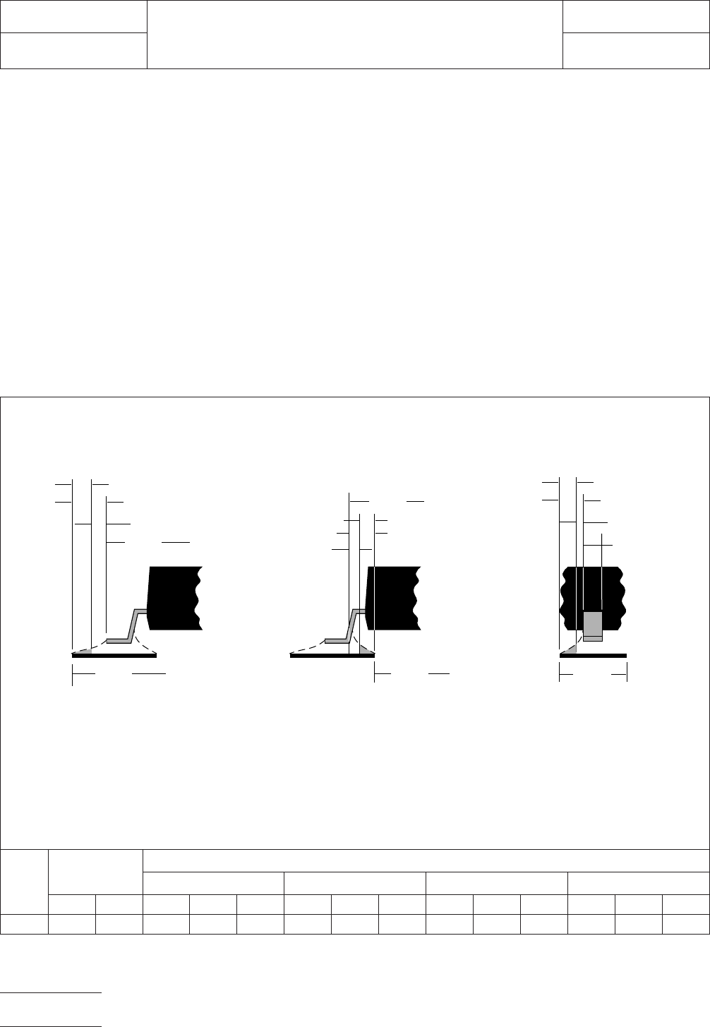
6.0 TOLERANCE AND SOLDER JOINT ANALYSIS
Figure 4 provides an analysis of tolerance assumptions and
resultant solder joints based on the land pattern dimensions
shown in Figure 3. Tolerances for the component dimensions,
the land pattern dimensions (fabrication tolerances on the
interconnecting substrate), and the component placement
equipment accuracy are all taken into consideration.
Figure 4 provides the solder joint minimums for toe, heel, and
side fillets, as discussed in Section 3.3. The tolerances are
addressed in a statistical mode, and assume even distribution
of the tolerances for component, fabrication, and placement
accuracy.
Individual tolerances for fabrication (‘‘F’’) and component
placement equipment accuracy (‘‘P’’) are assumed to be as
given in the table. These numbers may be modified based on
user equipment capability or fabrication criteria. Component
tolerance ranges (C
L
,C
S
, and C
W
) are derived by subtracting
minimum from maximum dimensions given in Figure 2. The
user may also modify these numbers, based on experience
with their suppliers. Modification of tolerances may result in
alternate land patterns (patterns with dimensions other than
the IPC registered land pattern dimensions).
The dimensions for minimum solder fillets at the toe, heel, or
side (J
T
,J
H
,J
S
) have been determined based on industry
empirical knowledge and reliability testing. Solder joint
strength is greatly determined by solder volume. An observ-
able solder fillet is necessary for evidence of proper wetting.
Thus, the values in the table usually provide for a positive sol-
der fillet. Nevertheless, the user may increase or decrease the
minimum value based on process capability.
RLP
No.
Tolerance
Assumptions
(mm)
Solder Joint
Toe (mm) Heel (mm) Side 1 (mm) Side 2 (mm)
FPC
L
J
T
min J
T
max C
S
H
H
min J
H
max C
W1
J
S1
min J
S1
max C
W2
J
S2
min J
S2
max
230 0.2 0.2 0.60 0.52 0.85 0.825 0.03 0.46 0.20 0.10 0.30 0.20 0.13 0.35
Figure 4 Tolerance and solder joint analysis
Zmax
Lmin
▼
▼
▼
▼
1
/2 T
T
J
T
min
Zmax = Lmin + 2J
T
min + T
T
Where:
J
T
min = Minimum toe fillet
T
T
= Combined tolerances
at toe fillet
Smax
J
H
min
Gmin = Smax - 2J
H
min - T
H
Where:
J
H
min = Minimum heel fillet
T
H
= Combined tolerances
at heel fillet
1
/2 T
H
Xmax
Xmax = Wmin + 2J
S
min + T
S
Where:
J
S
min = Minimum side fillet
T
S
= Combined tolerances
at side fillet
▼
▼
Toe Fillet
▼
▼
▼
Heel Fillet Side Fillet
▼
▼
▼
▼
▼
J
T
max
J
H
max
J
S
min
▼
▼
▼
▼
▼
▼
▼
▼
▼
▼
▼
▼
▼
▼
▼
Gmin
▼
1
/2 T
S
J
S
max
▼
▼
▼
Wmin
▼
IPC-782-8-10-4
IPC-SM-782
Subject
SOT 223
Date
8/93
Section
8.10
Revision
Page4of4
电子技术应用 www.ChinaAET.com
1.0 SCOPE
This subsection provides the component and land pattern
dimensions for TO 252 (small outline transistor) components.
Basic construction of the TO 252 device is also covered. At
the end of this subsection is a listing of the tolerances and
target solder joint dimensions used to arrive at the land pat-
tern dimensions.
2.0 APPLICABLE DOCUMENTS
See Section 8.0 for documents applicable to the subsections.
2.1 Electronic Industries Association (EIA)
JEDEC Pub-
lication 95 Registered and Standard Outlines for Solid State
and Related Products, TO-252, Issue ‘‘B’’ dated 9/88
Application for copies should be addressed to:
Global Engineering Documents
1990 M Street N.W.
Washington, DC
3.0 COMPONENT DESCRIPTIONS
These parts are for dual diodes and Darlington transistors.
3.1 Basic Construction
See Figure 1.
3.1.1 Termination Materials
Leads should be solder-
coated with a tin/lead alloy. The solder should contain
between 58 to 68% tin. Solder may be applied to the leads by
hot dipping or by plating from solution. Plated solder termina-
tions should be subjected to post-plating reflow operation to
fuse the solder. The tin/lead finish should be at least 0.0075
mm [0.0003 in] thick.
Solder finish applied over precious metal electrodes should
have a diffusion barrier layer between the electrode metalliza-
tion and the solder finish. The barrier layer should be nickel or
an equivalent diffusion barrier, and should be at least 0.00125
mm [0.00005 in] thick.
3.1.2 Marking
Parts are available with or without marked
values.
3.1.3 Carrier Package Format
Carrier package format
shall be according to the following: body type TO-252, 12 mm
tape/8 mm pitch.
3.1.4 Resistance to Soldering
Parts should be capable of
withstanding five cycles through a relow system operating at
215°C. Each cycle shall consist of 60 seconds exposure at
215°C. Parts must also be capable of withstanding a mini-
mum of 10 seconds immersion in molten solder at 260°C.
IPC-782-8-11-1
Figure 1 TO 252 construction
IPC-SM-782
Surface Mount Design
and Land Pattern Standard
Date
5/96
Section
8.11
Revision
A
Subject
TO 252/TO 268
Page1of4
电子技术应用 www.ChinaAET.com
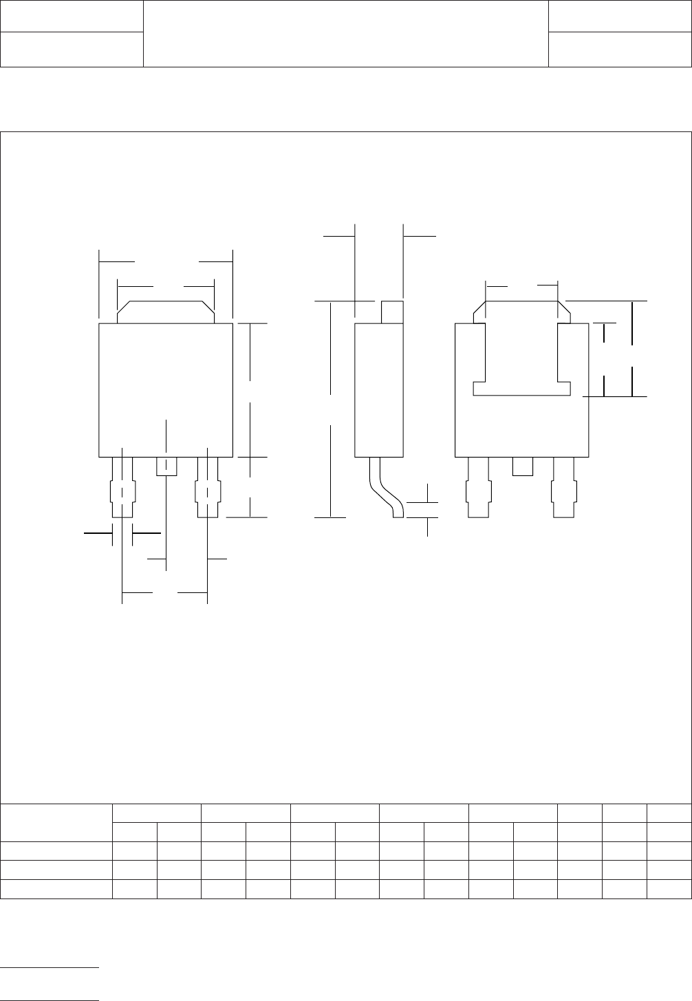
4.0 COMPONENT DIMENSIONS
Figure 2 provides the component dimensions for TO 252 components.
Component
Identifier
LW1W2T1T2P1P2H
min max min max min max min max min max basic basic max
TS-003* 9.32 10.41 0.64 0.91 4.35 5.35 0.51 0.80 4.00 5.50 2.28 4.57 2.38
TS-005** 14.60 15.88 0.51 0.91 6.22 6.86 2.29 2.79 8.00 9.00 2.54 5.08 4.83
TO 368 18.70 19.10 1.15 1.45 13.30 13.60 2.40 2.70 12.40 12.70 5.45 10.90 5.10
Figure 2 TO 252 component dimensions
*Formerly TO 252
**Formerly TO 263
6.35–6.73
▼
▼
▼
▼
▼
▼
▼
▼
▼
▼
W1
P2
▼
▼
L
▼
▼
H
▼
▼
4.32
MIN
T2
▼
▼
▼
▼
T1
W2
▼
▼
5.97–6.22
2.55–2.93
▼
▼
4.32
MIN
▼
▼
P1
IPC-782-8-11-2
IPC-SM-782
Subject
TO 252/TO 268
Date
5/96
Section
8.11
Revision
A
Page2of4
电子技术应用 www.ChinaAET.com