IPC-SM-782A 表面安装设计和焊盘设计标准(带BGA).pdf - 第116页
This Page Intentionally Left Blank IPC-SM-782 Subject Components with Gullwings on Two Sides Date 8/93 Section 9.0 Revision P a g e2o f2 电子技术应用 www.ChinaAET.com

1.0 INTRODUCTION
This section covers land patterns for
components with gullwings on two sides. Each subsection
contains information in accordance with the following format:
1.0 Scope
2.0 Applicable Documents
3.0 General Component Description (Figure 1)
4.0 Component Dimensions (Figure 2)
5.0 Land Pattern Dimensions (Figure 3)
6.0 Tolerance and Solder Joint Analysis (Figure 4)
The following is the table of contents for this section:
Table of Contents
Components with Gullwing Leads on Two Sides
Section Component Standard Source Lead Pitch
9.1 SOIC JEDEC 1.27 mm
9.2 SSOIC JEDEC 0.63 and
0.80 mm
9.3 SOPIC EIAJ 1.27 mm
9.4 TSOP EIAJ 0.3, 0.4,
0.5 mm
9.5 CFP 1.27 mm
2.0 APPLICABLE DOCUMENTS
The following documents, of the issue in effect on the revision
date of this section, form a part of this specification to the
extent specified herein.
2.1 Electronic Industries Association (EIA)
1
EIA-481-A
Taping of Surface Mount Components for Auto-
matic Placement
2.2 International Electrotechnical Commission (IEC)
2
IEC 97
Grid Elements
2.3 Electronic Industries Association of Japan
3
IC-74-1
General Rules for Preparation of Outline Drawings of
Integrated Circuits
IC-74-2
General Rules for Preparation of Outline Drawings of
Integrated Circuits, Thin Small Outline Packages
3.0 General Information
3.1 General Component Description
The two-sided gull
wing family has a number of generic package sizes in the
family. The body sizes are varied, but the basic family is char-
acterized by 1.27 mm or 0.63 mm lead centers with leads on
the long side of a rectangular body. The family has been
expanded to include a limited number of 0.80, 0.65, 0.50,
0.40, and 0.3 mm pitch devices.
Within the component families, body width and lead span are
constant, while body length changes as the lead count
changes.
A major advantage of this package style is that it can be pre-
tested prior to substrate assembly while still offering relatively
high density. Its small area, low height, and minimal weight are
its major advantages over DIPs. The package has orientation
features on the edge of the package to aid in handling and
identification.
Coplanarity is an issue for all components with gullwings on
two sides. In general, the leads must be coplanar within 0.1
mm. That is, when the component is placed on a flat surface,
(e.g., a granite block), no lead may be more than 0.1 mm off
the flat surface.
3.2 Process Considerations
Some members of the SOIC
family are processed on the secondary side and wave sol-
dered. When parts are processed by wave solder, correct part
orientation must be observed. Consult your manufacturer
before placing SOIC’s on the wave solder side of the board.
High lead count packages and fine pitch parts, 0.63 mm or
less, should be processed by infrared reflow, conduction
reflow, or hot bar soldering, and should not be wave soldered.
1. Application for copies of EIA and EIAJ documents should
be addressed to EIA, 2001 Pennsylvania Ave N.W., Wash-
ington, DC, 20006-1813 or Global Engineering Docu-
ments, 1990 M St. N.W., Washington, DC 20036.
2. Application for copies should be addressed to IEC, 3 rue
de Varembe, PO Box 131 - 1211 Geneva 20, Switzerland
IPC-SM-782
Surface Mount Design
and Land Pattern Standard
Date
8/93
Section
9.0
Revision Subject
Components with
Gullwings on Two Sides
Page1of2
电子技术应用 www.ChinaAET.com

This Page Intentionally Left Blank
IPC-SM-782
Subject
Components with Gullwings on Two Sides
Date
8/93
Section
9.0
Revision
Page2of2
电子技术应用 www.ChinaAET.com
1.0 SCOPE
This subsection provides the component and land pattern
dimensions for small outline integrated circuits (SOIC compo-
nents) with gullwing leads. Basic construction of the SOIC
device is also covered. At the end of this subsection is a list-
ing of the tolerances and target solder joint dimensions used
to arrive at the land pattern dimensions.
2.0 APPLICABLE DOCUMENTS
See Section 9.0 for documents applicable to the subsections.
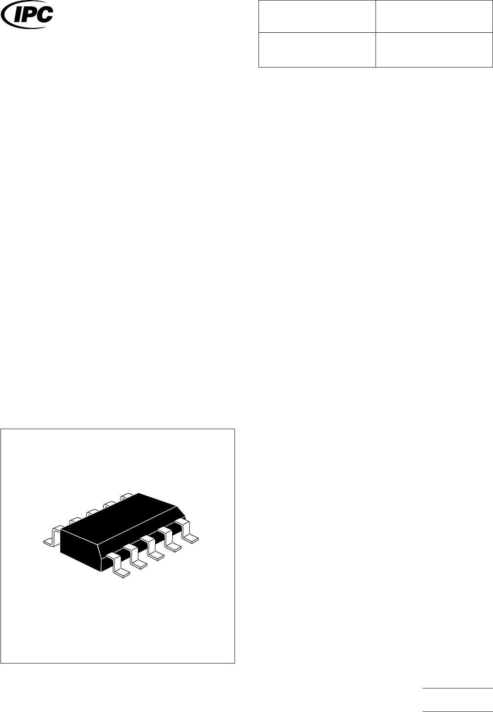
3.0 COMPONENT DESCRIPTIONS
These components are all on 1.27 mm pitch, and are available
in narrow body (3.90 mm), wide body (7.50 mm) and extra
wide body (8.90 mm) sizes, ranging from 8 to 36 pins.
3.1 Basic Construction
See Figure 1. Basic construction
consists of a plastic body and metallic leads.
3.1.1 Termination Materials
Leads should be solder-
coated with a tin/lead alloy. The solder should contain
between 58 to 68% tin. Solder may be applied to the termi-
nation by hot dipping or by plating from solution. Plated sol-
der terminations should be subjected to a post-plating reflow
operation to fuse the solder. The tin/lead finish should be at
least 0.00075 mm [0.0003 in] thick.
Solder finish applied over precious-metal leads shall have a
diffusion-barrier layer between the lead metallization and the
solder finish. The barrier layer should be nickel or an equiva-
lent diffusion barrier, and should be at least 0.00125 mm
[0.00005 in] thick.
3.1.2 Marking
All parts shall be marked with a part number
and ‘‘Pin 1’’ location. ‘‘Pin 1’’ location may be molded into the
plastic body.
3.1.3 Carrier Package Format
Bulk rods, 24 mm tape/
8–12 mm pitch is preferred for best handling. Tube carriers
are also used.
3.1.4 Resistance to Soldering
Parts should be capable of
withstanding ten cycles through a standard reflow system
operating at 215°C. Each cycle shall consist of 60 seconds
exposure at 215°C. Parts must also be capable of withstand-
ing a minimum of 10 seconds immersion in molten solder at
260°C.
IPC-782-9-1-1
Figure 1 SOIC construction
IPC-SM-782
Surface Mount Design
and Land Pattern Standard
Date
5/96
Section
9.1
Revision
A
Subject
SOIC
Page1of4
电子技术应用 www.ChinaAET.com