IPC-SM-782A 表面安装设计和焊盘设计标准(带BGA).pdf - 第125页
1.0 SCOPE This subsection provides component and land pattern dimen- sions for small outline packages (SOP components) with gull- wing leads on two sides. Basic construction of the SOP device is also covered. At the end …
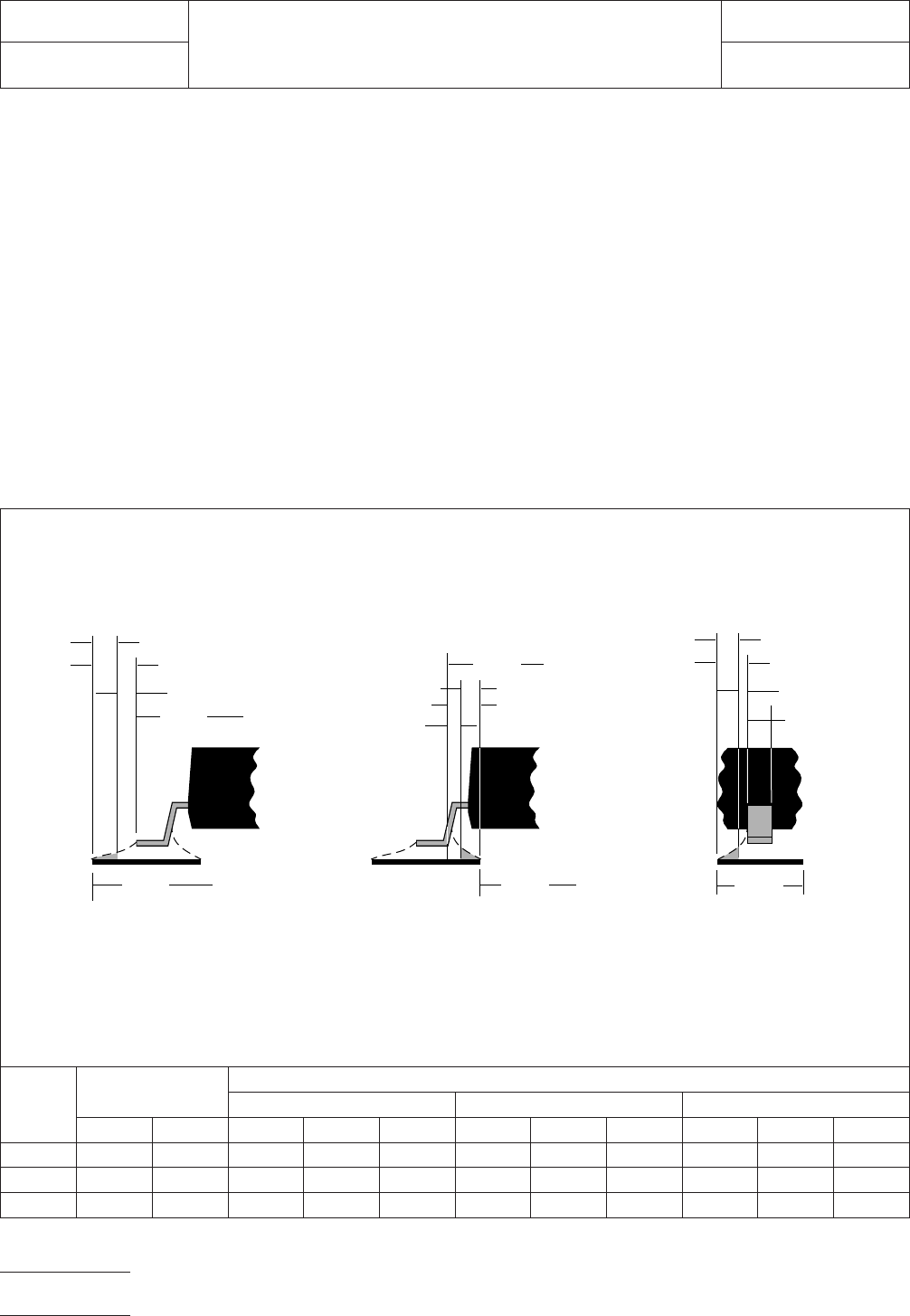
6.0 TOLERANCE AND SOLDER JOINT ANALYSIS
Figure 4 provides an analysis of tolerance assumptions and
resultant solder joints based on the land pattern dimensions
shown in Figure 3. Tolerances for the component dimensions,
the land pattern dimensions (fabrication tolerances on the
interconnecting substrate), and the component placement
equipment accuracy are all taken into consideration.
Figure 4 provides the solder joint minimums for toe, heel, and
side fillets, as discussed in Section 3.3. The tolerances are
addressed in a statistical mode, and assume even distribution
of the tolerances for component, fabrication, and placement
accuracy.
Individual tolerances for fabrication (‘‘F’’) and component
placement equipment accuracy (‘‘P’’) are assumed to be as
given in the table. These numbers may be modified based on
user equipment capability or fabrication criteria. Component
tolerance ranges (C
L
,C
S
, and C
W
) are derived by subtracting
minimum from maximum dimensions given in Figure 2. The
user may also modify these numbers, based on experience
with their suppliers. Modification of tolerances may result in
alternate land patterns (patterns with dimensions other than
the IPC registered land pattern dimensions).
The dimensions for minimum solder fillets at the toe, heel, or
side (J
T
,J
H
,J
S
) have been determined based on industry
empirical knowledge and reliability testing. Solder joint
strength is greatly determined by solder volume. An observ-
able solder fillet is necessary for evidence of proper wetting.
Thus, the values in the table usually provide for a positive sol-
der fillet. Nevertheless, the user may increase or decrease the
minimum value based on process capability.
RLP No.
Tolerance
Assumptions (mm)
Solder Joint
Toe (mm) Heel (mm) Side (mm)
FPC
L
T
T
min J
T
max C
S
J
H
min J
H
max C
W
J
S
min J
S
max
330A 0.10 0.10 0.64 0.46 0.79 0.96 0.39 0.88 0.10 0.01 0.10
331A 0.10 0.10 0.64 0.46 0.79 0.96 0.39 0.88 0.10 0.01 0.10
332A 0.10 0.10 0.50 0.44 0.70 0.65 0.49 0.82 0.15 0.00 0.10
Figure 4 Tolerance and solder joint analysis
Zmax
Lmin
▼
▼
▼
▼
1
/2 T
T
J
T
min
Zmax = Lmin + 2J
T
min + T
T
Where:
J
T
min = Minimum toe fillet
T
T
= Combined tolerances
at toe fillet
Smax
J
H
min
Gmin = Smax - 2J
H
min - T
H
Where:
J
H
min = Minimum heel fillet
T
H
= Combined tolerances
at heel fillet
1
/2 T
H
Xmax
Xmax = Wmin + 2J
S
min + T
S
Where:
J
S
min = Minimum side fillet
T
S
= Combined tolerances
at side fillet
▼
▼
Toe Fillet
▼
▼
▼
Heel Fillet Side Fillet
▼
▼
▼
▼
▼
J
T
max
J
H
max
J
S
min
▼
▼
▼
▼
▼
▼
▼
▼
▼
▼
▼
▼
▼
▼
▼
Gmin
▼
1
/2 T
S
J
S
max
▼
▼
▼
Wmin
▼
IPC-782-9-2-4
IPC-SM-782
Subject
SSOIC
Date
5/96
Section
9.2
Revision
A
Page4of4
电子技术应用 www.ChinaAET.com
1.0 SCOPE
This subsection provides component and land pattern dimen-
sions for small outline packages (SOP components) with gull-
wing leads on two sides. Basic construction of the SOP
device is also covered. At the end of this subsection is a list-
ing of the tolerances and target solder joint dimensions used
to arrive at the land pattern dimensions.
2.0 APPLICABLE DOCUMENTS
See Section 9.0 and the following for documents applicable to
this subsection.
2.1 Electronic Industries Association of Japan (EIAJ)
EIAJ-7402-1
General Rules for the Preparation of Outine
Drawings of Integrated Circuits Small Outline Packages
3.0 COMPONENT DESCRIPTIONS
3.1 Basic Construction
IPC-SM-782 has defined center-
to-center spacing for the land pattern slightly differently than is
indicated in the EIAJ specification ED 7402-1.
This specification allows for 6 families of the SOP. EIAJ clas-
sifies the families by the center-to-center distance of the land
patterns and the outer extremities of the leads (dimension ‘‘L’’
in IPC-SM-782). The basic construction of the SOP specified
by EIAJ is the same construction as for SOIC specified by
JEDEC. Both have gullwing leads on 1.27 mm centers.
The EIAJ specification allows for a number of positions of the
components to be in any of the families (e.g., body width). The
sizes shown in Figure 2 are the most common, however, there
are Type II SOP 14s and there are also Type I SOP 16s. See
Figure 2.
3.1.1 Termination Materials
Leads must be solder-
coated with a tin/lead alloy. The solder should contain
between 58 to 68% tin. Solder may be applied to the leads by
hot dipping or by plating from solution. Plated solder termina-
tions should be subjected to post-plating reflow operation to
fuse the solder. The tin/lead finish should be at least 0.0075
mm [0.0003 in] thick.
3.1.2 Marking
Parts are available with or without part
number markings. Usually an index mark indicates pin 1.
3.1.3 Carrier Package Format
Bulk rods, 24 mm tape/
8–12 mm pitch is preferred for best handling. Tube carriers
are also used.
3.1.4 Resistance to Solder Parts should be capable of
withstanding ten cycles through a standard reflow system
operating at 215°C. Each cycle shall consist of 60 seconds
exposure at 215°C. Parts must also be capable of withstand-
ing a minimum of 10 seconds immersion in molten solder at
260°C.
IPC-782-9-3-1
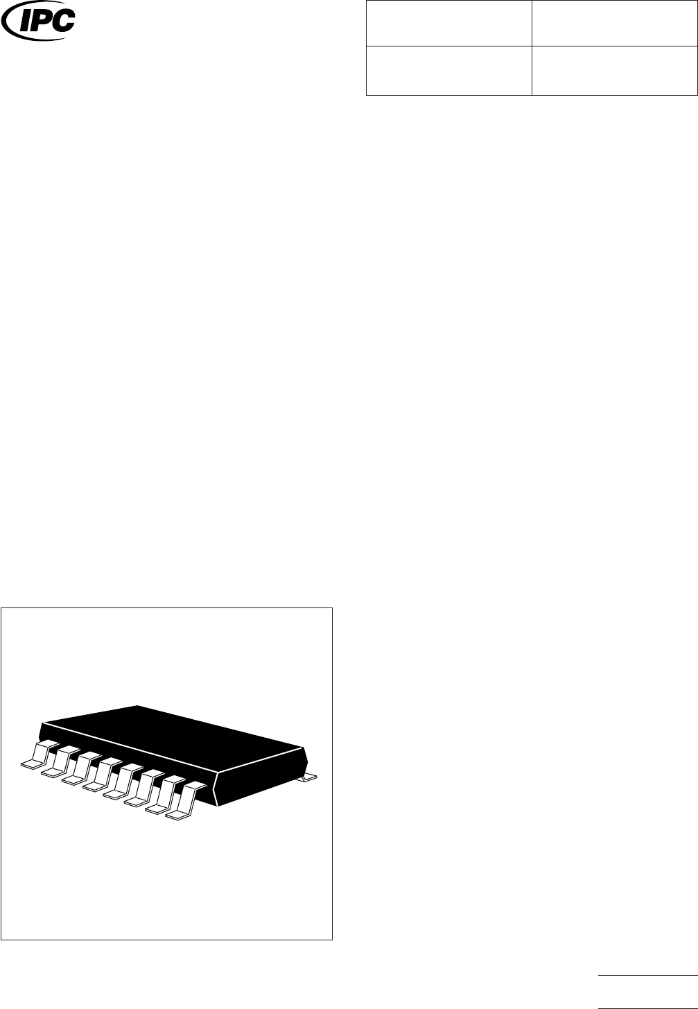
Figure 1 SOPIC construction
IPC-SM-782
Surface Mount Design
and Land Pattern Standard
Date
5/96
Section
9.3
Revision
A
Subject
SOP
Page1of4
电子技术应用 www.ChinaAET.com
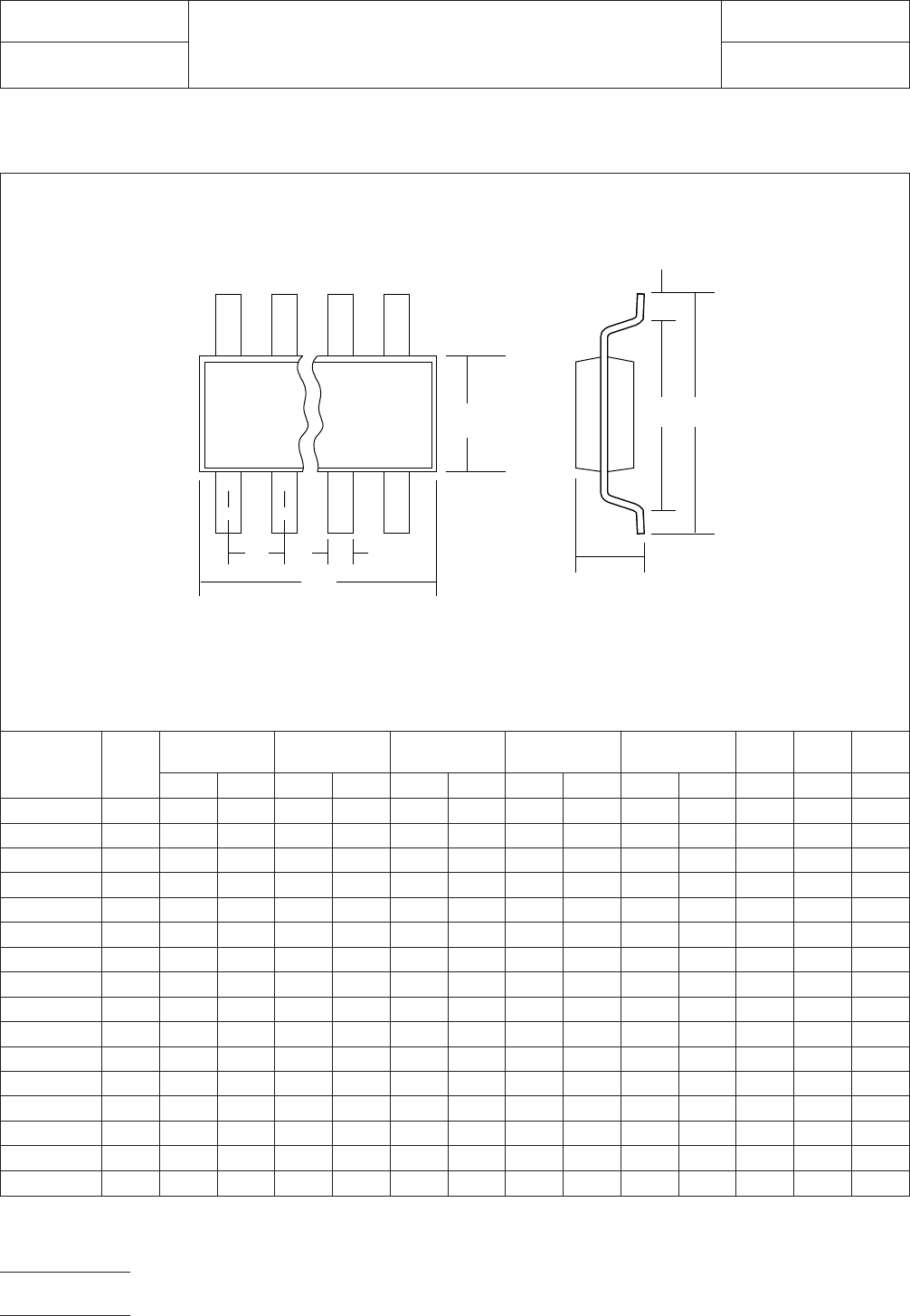
4.0 COMPONENT DIMENSIONS
Figure 2 provides the component dimensions for SOPIC components.
Component
Identifier
(mm) Type
L (mm) S (mm) W (mm) T (mm) A (mm)
B
(mm)
H
(mm)
P
(mm)
min max min max min max min max min max max max basic
SOP 6 I 5.72 6.99 3.72 5.11 0.35 0.51 0.60 1.00 3.92 4.72 6.35 1.5 1.27
SOP 8 I 5.72 6.99 3.72 5.11 0.35 0.51 0.60 1.00 3.92 4.72 6.35 1.5 1.27
SOP 10 I 5.72 6.99 3.72 5.11 0.35 0.51 0.60 1.00 3.92 4.72 8.89 1.5 1.27
SOP 12 I 5.72 6.99 3.72 5.11 0.35 0.51 0.60 1.00 3.92 4.72 8.89 1.5 1.27
SOP 14 I 5.72 6.99 3.72 5.11 0.35 0.51 0.60 1.00 3.92 4.72 11.43 1.5 1.27
SOP 16 II 7.62 8.89 5.62 7.01 0.35 0.51 0.60 1.00 5.02 6.22 11.43 2.0 1.27
SOP 18 II 7.62 8.89 5.62 7.01 0.35 0.51 0.60 1.00 5.02 6.22 13.97 2.0 1.27
SOP 20 II 7.62 8.89 5.62 7.01 0.35 0.51 0.60 1.00 5.02 6.22 13.97 2.0 1.27
SOP 22 III 9.53 10.80 7.53 8.92 0.35 0.51 0.60 1.00 6.33 8.13 16.51 2.5 1.27
SOP 24 III 9.53 10.80 7.53 8.92 0.35 0.51 0.60 1.00 6.33 8.13 16.51 2.5 1.27
SOP 28 IV 11.43 12.70 9.43 10.82 0.35 0.51 0.60 1.00 8.23 10.03 19.05 3.0 1.27
SOP 30 IV 11.43 12.70 9.43 10.82 0.35 0.51 0.60 1.00 8.23 10.03 21.59 3.0 1.27
SOP 32 V 13.34 14.61 11.34 12.73 0.35 0.51 0.60 1.00 10.14 11.94 21.59 3.5 1.27
SOP 36 V 13.34 14.61 11.34 12.73 0.36 0.51 0.60 1.00 10.14 11.94 24.13 3.5 1.27
SOP 40 VI 15.24 16.51 13.24 14.63 0.35 0.51 0.60 1.00 12.04 13.84 27.94 4.0 1.27
SOP 42 VI 15.24 16.51 13.24 14.63 0.35 0.51 0.60 1.00 12.04 13.84 27.94 4.0 1.27
Figure 2 SOPIC component dimensions
▼
▼
▼
▼
▼
▼
B
PW
A
▼
▼
H
▼
▼
SL
▼
▼
▼
▼
▼
T
IPC-782-9-3-2
IPC-SM-782
Subject
SOP
Date
5/96
Section
9.3
Revision
A
Page2of4
电子技术应用 www.ChinaAET.com