IPC-SM-782A 表面安装设计和焊盘设计标准(带BGA).pdf - 第129页
1.0 SCOPE This subsection provides the component and land pattern dimensions for thin small outline packages (TSOP compo- nents) with gullwing leads on two sides. Basic construction of the TSOP device is also covered. At…
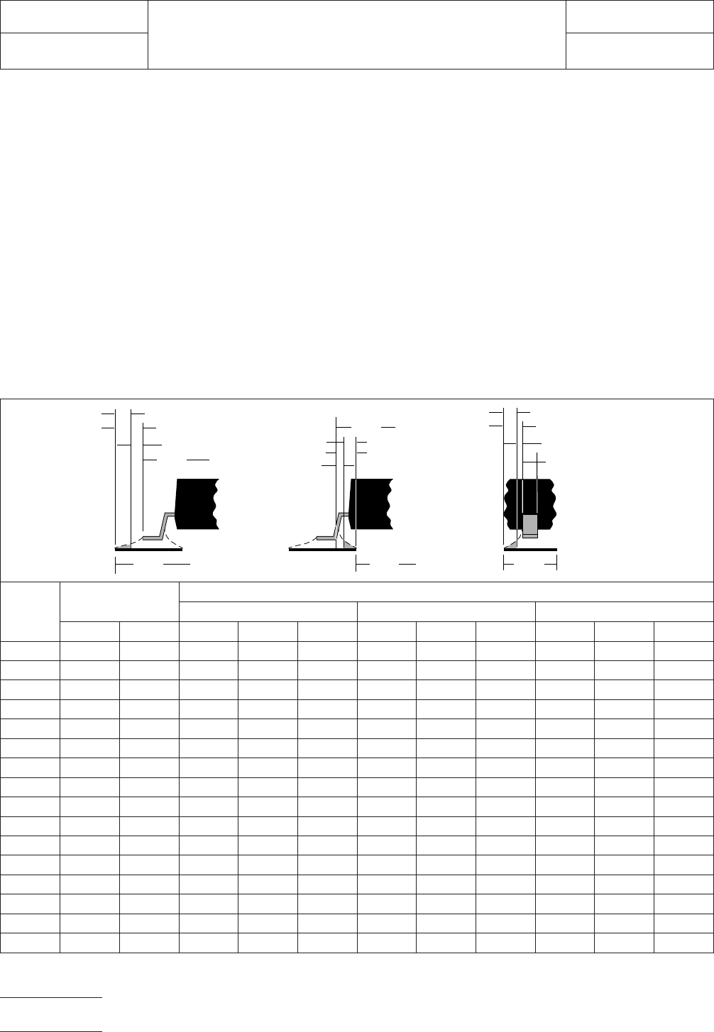
6.0 TOLERANCE AND SOLDER JOINT ANALYSIS
Figure 4 provides an analysis of tolerance assumptions and
resultant solder joints based on the land pattern dimensions
shown in Figure 3. Tolerances for the component dimensions,
the land pattern dimensions (fabrication tolerances on the
interconnecting substrate), and the component placement
equipment accuracy are all taken into consideration.
Figure 4 provides the solder joint minimums for toe, heel, and
side fillets, as discussed in Section 3.3. The tolerances are
addressed in a statistical mode, and assume even distribution
of the tolerances for component, fabrication, and placement
accuracy.
Individual tolerances for fabrication (‘‘F’’) and component
placement equipment accuracy (‘‘P’’) are assumed to be as
given in the table. These numbers may be modified based on
user equipment capability or fabrication criteria. Component
tolerance ranges (C
L
,C
S
, and C
W
) are derived by subtracting
minimum from maximum dimensions given in Figure 2. The
user may also modify these numbers, based on experience
with their suppliers. Modification of tolerances may result in
alternate land patterns (patterns with dimensions other than
the IPC registered land pattern dimensions).
The dimensions for minimum solder fillets at the toe, heel, or
side (J
T
,J
H
,J
S
) have been determined based on industry
empirical knowledge and reliability testing. Solder joint
strength is greatly determined by solder volume. An observ-
able solder fillet is necessary for evidence of proper wetting.
Thus, the values in the table usually provide for a positive sol-
der fillet. Nevertheless, the user may increase or decrease the
minimum value based on process capability.
RLP No.
Tolerance
Assumptions (mm)
Solder Joint
Toe (mm) Heel (mm) Side (mm)
FPC
L
J
T
min J
T
max C
S
J
H
min J
H
max C
W
J
S
min J
S
max
360A 0.10 0.10 1.27 0.20 0.84 1.26 0.36 1.06 0.16 0.02 0.13
361A 0.10 0.10 1.27 0.20 0.84 1.26 0.36 1.06 0.16 0.02 0.13
362A 0.10 0.10 1.27 0.20 0.84 1.26 0.36 1.06 0.16 0.02 0.13
363A 0.10 0.10 1.27 0.20 0.84 1.26 0.36 1.06 0.16 0.02 0.13
364A 0.10 0.10 1.27 0.20 0.84 1.26 0.36 1.06 0.16 0.02 0.13
365A 0.10 0.10 1.27 0.25 0.89 1.26 0.31 1.01 0.16 0.02 0.13
366A 0.10 0.10 1.27 0.25 0.89 1.26 0.31 1.01 0.16 0.02 0.13
367A 0.10 0.10 1.27 0.25 0.89 1.26 0.31 1.01 0.16 0.02 0.13
368A 0.10 0.10 1.27 0.20 0.84 1.26 0.36 1.06 0.16 0.02 0.13
369A 0.10 0.10 1.27 0.20 0.84 1.26 0.36 1.06 0.16 0.02 0.13
370A 0.10 0.10 1.27 0.25 0.89 1.26 0.31 1.01 0.16 0.02 0.13
371A 0.10 0.10 1.27 0.25 0.89 1.26 0.31 1.01 0.16 0.02 0.13
372A 0.10 0.10 1.27 0.19 0.83 1.26 0.37 1.07 0.16 0.02 0.13
373A 0.10 0.10 1.27 0.19 0.83 1.26 0.37 1.07 0.16 0.02 0.13
374A 0.10 0.10 1.27 0.24 0.88 1.26 0.32 1.02 0.16 0.02 0.13
375A 0.10 0.10 1.27 0.24 0.88 1.26 0.32 1.02 0.16 0.02 0.13
Figure 4 Tolerance and solder joint analysis
Zmax
Lmin
▼
▼
▼
▼
1
/2 T
T
J
T
min
Smax
J
H
min
1
/2 T
H
Xmax
▼
▼
Toe Fillet
▼
▼
▼
Heel Fillet
Side Fillet
▼
▼
▼
▼
▼
J
T
max
J
H
max
J
S
min
▼
▼
▼
▼
▼
▼
▼
▼
▼
▼
▼
▼
▼
▼
▼
Gmin
▼
1
/2 T
S
J
S
max
▼
▼
▼
Wmin
▼
IPC-782-9-3-4
IPC-SM-782
Subject
SOP
Date
5/96
Section
9.3
Revision
A
Page4of4
电子技术应用 www.ChinaAET.com
1.0 SCOPE
This subsection provides the component and land pattern
dimensions for thin small outline packages (TSOP compo-
nents) with gullwing leads on two sides. Basic construction of
the TSOP device is also covered. At the end of this subsec-
tion is a listing of the tolerances and target solder joint dimen-
sions used to arrive at the land pattern dimensions.
2.0 APPLICABLE DOCUMENTS
See Section 9.0 and the following for documents applicable to
this subsection.
2.1 Electronic Industries Association of Japan (EIAJ)
EIAJ-ED-7402-3
General Rules for the Preparation of Outline
Drawings of Integrated Circuits Thin Small Outline Packages
3.0 COMPONENT DESCRIPTIONS
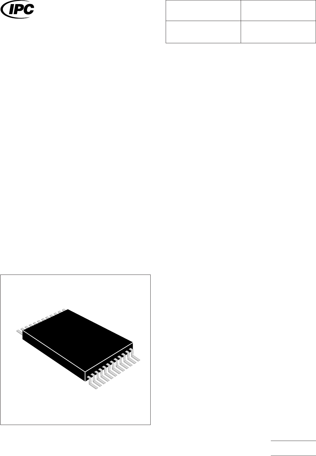
3.1 Basic Construction
The TSOP package is unique
among the component families of this section becaue its leads
protrude from the short side of the plastic body. The TSOP
components are available in four different pitches: 0.3, 0.4,
0.5, and 0.65 mm. They are typically specified by their two
largest dimensions—the plastic body size (in the short dimen-
sion), and the nominal toe-to-toe length (in the long dimen-
sion). Their use has grown because their height (less than
1.27 mm) allows them to be used in memory card technology.
EIAJ ED-7402-3 outlines sixteen different body sizes with pin
counts ranging from 16–76 pins. In general, as the long
dimension increases, the pitch decreases. See Figure 1.
3.1.1 Termination Materials
Leads must be solder-
coated with a tin/lead alloy. The solder should contain
between 58 to 68% tin. Solder may be applied to the leads by
hot dipping or by plating from solution. Plated solder termina-
tions should be subjected to post-plating reflow operation to
fuse the solder. The tin/lead finish should be at least 0.0075
mm [0.0003 in] thick.
3.1.2 Marking
Parts are available with or without part num-
ber markings. Usually an index mark indicates pin 1.
3.1.3 Carrier Packages Format
Trays are usually used for
handling TSOP’s.
3.1.4 Resistance to Soldering
Parts should be capable of
withstanding ten cycles through a standard reflow system
operating at 215°C. Each cycle shall consist of 60 seconds
exposure at 215°C. Parts must also be capable of withstand-
ing a minimum of 10 seconds immersion in molten solder at
260°C.
IPC-782-9-4-1
Figure 1 TSOP construction
IPC-SM-782
Surface Mount Design
and Land Pattern Standard
Date
5/96
Section
9.4
Revision
A
Subject
TSOP
Page1of4
电子技术应用 www.ChinaAET.com
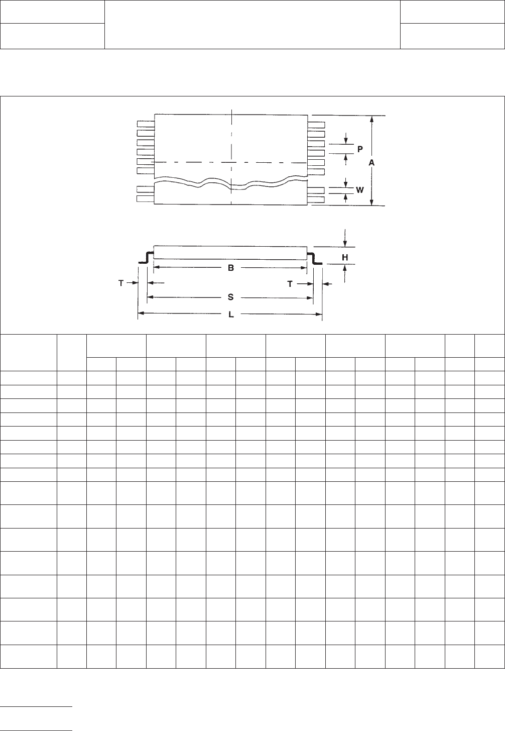
4.0 COMPONENT DIMENSIONS
Figure 2 provides the component dimensions for TSOP components.
Component
Identifier
(mm)
Pin
Count
L (mm) S (mm) W (mm) T (mm) A (mm) B (mm)
H
(mm)
P
(mm)
min max min max min max m in max min max min max max basic
TSOP 6x14 16 13.80 14.20 12.40 12.98 0.20 0.40 0.40 0.70 5.80 6.20 12.20 12.60 1.27 0.65
TSOP 6x16 24 15.80 16.20 14.40 14.98 0.10 0.30 0.40 0.70 5.80 6.20 14.20 14.60 1.27 0.50
TSOP 6x18 28 17.80 18.20 16.40 16.78 0.05 0.22 0.40 0.70 5.80 6.20 16.20 16.60 1.27 0.40
TSOP 6x20 36 19.80 20.20 18.40 18.98 0.05 0.15 0.40 0.70 5.80 6.20 18.20 18.60 1.27 0.30
TSOP 8x14 24 13.80 14.20 12.40 12.98 0.20 0.40 0.40 0.70 7.80 8.20 12.20 12.60 1.27 0.65
TSOP 8x16 32 15.80 16.20 14.40 14.98 0.10 0.30 0.40 0.70 7.80 8.20 14.20 14.60 1.27 0.50
TSOP 8x18 40 17.80 18.20 16.40 16.98 0.05 0.22 0.40 0.70 7.80 8.20 16.20 16.60 1.27 0.40
TSOP 8x20 52 19.80 20.20 18.40 18.98 0.05 0.15 0.40 0.70 7.80 8.20 18.20 18.60 1.27 0.30
TSOP
10x14
28 13.80 14.20 12.40 12.98 0.20 0.40 0.40 0.70 9.80 10.20 12.20 12.60 1.27 0.65
TSOP
10x16
40 15.80 16.20 14.40 14.98 0.10 0.30 0.40 0.70 9.80 10.20 14.20 14.60 1.27 0.50
TSOP
10x18
48 17.80 18.20 16.40 16.98 0.05 0.22 0.40 0.70 9.80 10.20 16.20 16.60 1.27 0.40
TSOP
10x20
64 19.80 20.20 18.40 18.98 0.05 0.15 0.40 0.70 9.80 10.20 18.20 18.60 1.27 0.30
TSOP
12x14
36 13.80 14.20 12.40 12.98 0.20 0.40 0.40 0.70 11.80 12.20 12.20 12.60 1.27 0.65
TSOP
12x16
48 15.80 16.20 14.40 14.98 0.10 0.30 0.40 0.70 11.80 12.20 14.20 14.60 1.27 0.50
TSOP
12x18
60 17.80 18.20 16.40 16.98 0.05 0.22 0.40 0.70 11.80 12.20 16.20 16.60 1.27 0.40
TSOP
12x20
76 19.80 20.20 18.40 18.98 0.05 0.15 0.40 0.70 11.80 12.20 18.20 18.60 1.27 0.30
Figure 2 TSOP component dimensions
IPC-782-9-4-2
IPC-SM-782
Subject
TSOP
Date
5/96
Section
9.4
Revision
A
Page2of4
电子技术应用 www.ChinaAET.com