IPC-SM-782A 表面安装设计和焊盘设计标准(带BGA).pdf - 第133页
1.0 SCOPE This subsection provides the component and land pattern dimensions for ceramic flat packs (CFP components) with gullwing leads on two sides. Basic construction of the CFP device is also covered. At the end of t…
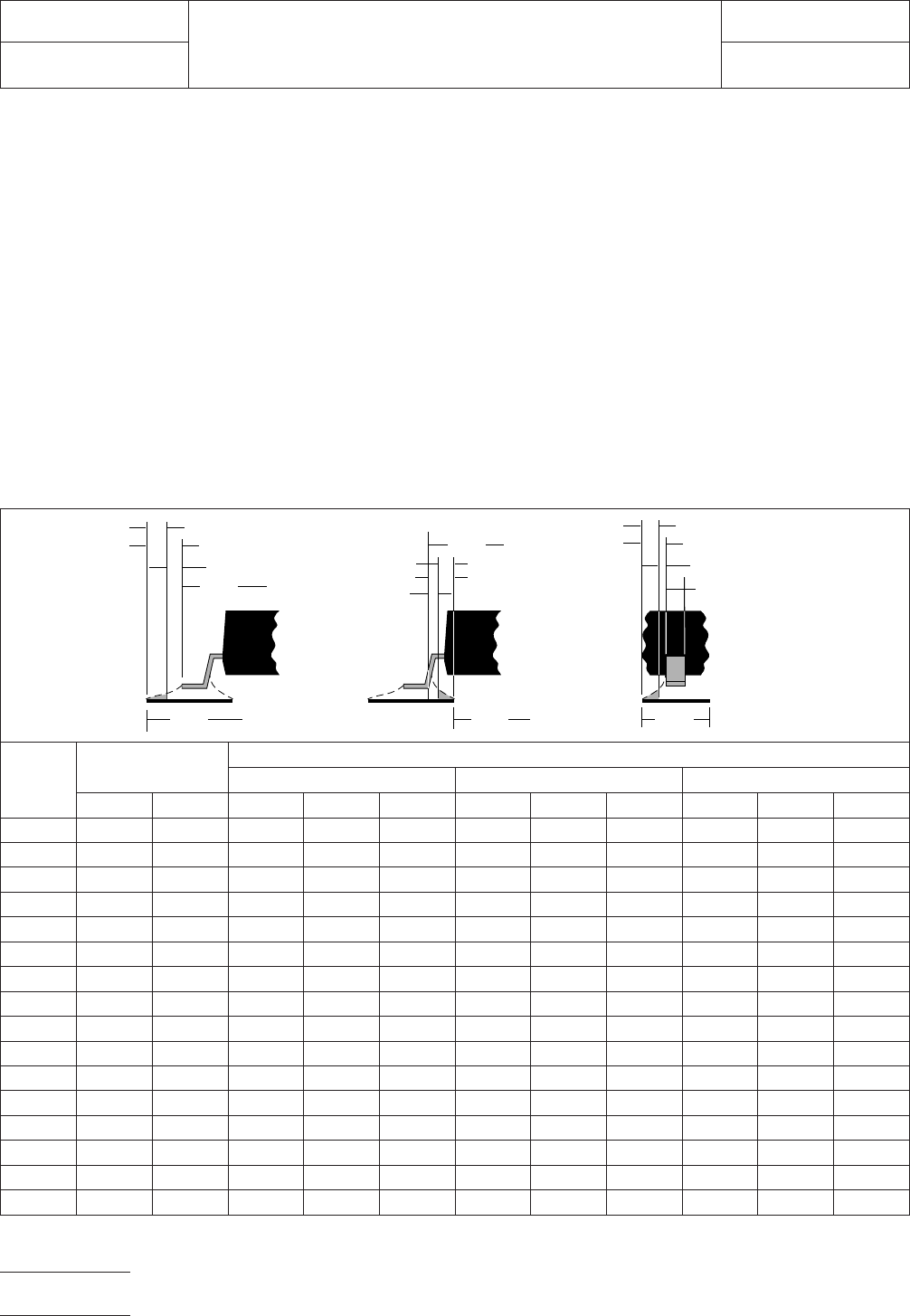
6.0 TOLERANCE AND SOLDER JOINT ANALYSIS
Figure 4 provides an analysis of tolerance assumptions and
resultant solder joints based on the land pattern dimensions
shown in Figure 3. Tolerances for the component dimensions,
the land pattern dimensions (fabrication tolerances on the
interconnecting substrate), and the component placement
equipment accuracy are all taken into consideration.
Figure 4 provides the solder joint minimums for toe, heel, and
side fillets, as discussed in Section 3.3. The tolerances are
addressed in a statistical mode, and assume even distribution
of the tolerances for component, fabrication, and placement
accuracy.
Individual tolerances for fabrication (‘‘F’’) and component
placement equipment accuracy (‘‘P’’) are assumed to be as
given in the table. These numbers may be modified based on
user equipment capability or fabrication criteria. Component
tolerance ranges (C
L
,C
S
, and C
W
) are derived by subtracting
minimum from maximum dimensions given in Figure 2. The
user may also modify these numbers, based on experience
with their suppliers. Modification of tolerances may result in
alternate land patterns (patterns with dimensions other than
the IPC registered land pattern dimensions).
The dimensions for minimum solder fillets at the toe, heel, or
side (J
T
,J
H
,J
S
) have been determined based on industry
empirical knowledge and reliability testing. Solder joint
strength is greatly determined by solder volume. An observ-
able solder fillet is necessary for evidence of proper wetting.
Thus, the values in the table usually provide for a positive sol-
der fillet. Nevertheless, the user may increase or decrease the
minimum value based on process capability.
RLP No.
Tolerance
Assumptions (mm)
Solder Joint
Toe (mm) Heel (mm) Side (mm)
FPC
L
J
T
min J
T
max C
S
J
H
min J
H
max C
W
J
S
min J
S
max
390A 0.10 0.10 0.40 0.29 0.50 0.58 0.39 0.69 0.20 -0.02 0.10
391A 0.10 0.10 0.40 0.29 0.50 0.58 0.39 0.69 0.20 -0.02 0.10
392A 0.10 0.10 0.40 0.29 0.50 0.58 0.39 0.69 0.10 -0.01 0.10
393A 0.10 0.10 0.40 0.29 0.50 0.58 0.39 0.69 0.06 -0.03 0.06
394A 0.10 0.10 0.40 0.29 0.50 0.58 0.39 0.69 0.20 -0.02 0.10
395A 0.10 0.10 0.40 0.29 0.50 0.58 0.39 0.69 0.20 -0.02 0.10
396A 0.10 0.10 0.40 0.29 0.50 0.58 0.39 0.69 0.17 -0.01 0.10
397A 0.10 0.10 0.40 0.29 0.50 0.58 0.39 0.69 0.10 -0.03 0.06
398A 0.10 0.10 0.40 0.29 0.50 0.58 0.39 0.69 0.20 -0.02 0.10
399A 0.10 0.10 0.40 0.29 0.50 0.58 0.39 0.69 0.20 -0.02 0.10
400A 0.10 0.10 0.40 0.29 0.50 0.58 0.39 0.69 0.17 -0.01 0.10
401A 0.10 0.10 0.40 0.29 0.50 0.58 0.39 0.69 0.10 -0.03 0.06
402A 0.10 0.10 0.40 0.29 0.50 0.58 0.39 0.69 0.20 -0.02 0.10
403A 0.10 0.10 0.40 0.29 0.50 0.58 0.39 0.69 0.20 -0.02 0.10
404A 0.10 0.10 0.40 0.29 0.50 0.58 0.39 0.69 0.17 -0.01 0.10
405A 0.10 0.10 0.40 0.29 0.50 0.58 0.39 0.69 0.10 -0.03 0.06
Figure 4 Tolerance and solder joint analysis
Zmax
Lmin
▼
▼
▼
▼
1
/2 T
T
J
T
min
Smax
J
H
min
1
/2 T
H
Xmax
▼
▼
Toe Fillet
▼
▼
▼
Heel Fillet
Side Fillet
▼
▼
▼
▼
▼
J
T
max
J
H
max
J
S
min
▼
▼
▼
▼
▼
▼
▼
▼
▼
▼
▼
▼
▼
▼
▼
Gmin
▼
1
/2 T
S
J
S
max
▼
▼
▼
Wmin
▼
IPC-782-9-4-4
IPC-SM-782
Subject
TSOP
Date
5/96
Section
9.4
Revision
A
Page4of4
电子技术应用 www.ChinaAET.com
1.0 SCOPE
This subsection provides the component and land pattern
dimensions for ceramic flat packs (CFP components) with
gullwing leads on two sides. Basic construction of the CFP
device is also covered. At the end of this subsection is a list-
ing of the tolerances and target solder joint dimensions used
to arrive at the land pattern dimensions.
2.0 APPLICABLE DOCUMENTS
See Section 9.0 and the following for documents applicable to
this subsection.
JEDEC Publication 95
Registered and Standard Outlines for
Solid State and Related Products:
Outline Issues Title
MO-003 C Flatpack Family, 5.08 Width, 1.27
Pitch
MO-004 C Flatpack Family, 7.62 Width, 1.27
Pitch
MO-018 — Flatpack Family, 10.16 Width,
1.27 Pitch
MO-019 D Flatpack Family, 10.16 Width,
1.27 Pitch
MO-020 C Flatpack Family, 12.70 Width,
1.27 Pitch
MO-021 C Flatpack Family, 15.24 Width,
1.27 Pitch
MO-022 D Flatpack Family, 17.78 Width,
1.27 Pitch
MO-023 C Flatpack Family, 22.86 Width,
1.27 Pitch
Application for copies should be addressed to:
Global Engineering Documents
1990 M Street N.W.
Washington, DC
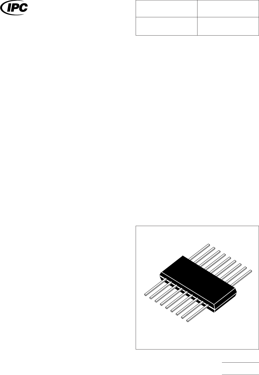
3.0 COMPONENT DESCRIPTIONS
3.1 Basic Construction
See Figure 1. Basic construction
consists of a ceramic body and metallic leads. Leads are
trimmed and formed into gullwing shape as shown in Figure 2.
3.1.1 Termination Materials
Leads should be solder-
coated with a tin/lead alloy. The solder should contain
between 58 to 68% tin. Solder may be applied to the termi-
nation by hot dipping or by plating from solution. Plated sol-
der terminations should be subjected to a post-plating reflow
operation to fuse the solder. The tin/lead finish should be at
least 0.00075 mm [0.0003 in] thick.
3.1.2 Marking
All parts shall be marked with a part num-
ber and an index area. The index area shall identify the loca-
tion of pin 1.
3.1.3
Carrier trays are used for handling CFPs.
3.1.4 Resistance to Soldering
Parts should be capable of
withstanding ten cycles through a standard reflow system
operating at 215°C. Each cycle shall consist of 60 seconds
exposure at 215°C. Parts must also be capable of withstand-
ing a minimum of 10 seconds immersion in molten solder at
260°C.
IPC-782-9-5-1
Figure 1 CFP construction
IPC-SM-782
Surface Mount Design
and Land Pattern Standard
Date
8/93
Section
9.5
Revision Subject
CFP
Page1of4
电子技术应用 www.ChinaAET.com
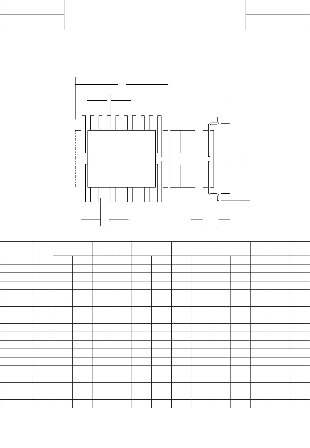
4.0 COMPONENT DIMENSIONS
Figure 2 provides the component dimensions for CFP components.
CFP
Component
Identifier
Pin
Count
L (mm) S (mm) W (mm) T (mm) A (mm)
B
(mm)
H
(mm) E
min max min max min max min max min max max max basic
MO-003 10 9.00 9.60 6.46 7.26 0.25 0.35 0.90 1.27 2.54 5.08 7.36 2.50 1.27
MO-003 14 9.00 9.60 6.46 7.26 0.25 0.35 0.90 1.27 2.54 5.08 9.90 2.50 1.27
MO-004 10 11.00 11.60 8.46 9.26 0.38 0.48 0.90 1.27 5.08 7.62 7.36 2.50 1.27
MO-004 14 11.00 11.60 8.46 9.26 0.38 0.48 0.90 1.27 5.08 7.62 9.90 2.50 1.27
MO-004 16 11.00 11.60 8.46 9.26 0.38 0.48 0.90 1.27 5.08 7.62 11.17 2.50 1.27
MO-018 20 11.00 11.60 8.46 9.26 0.25 0.35 0.90 1.27 7.62 10.16 13.71 2.50 1.27
MO-019 24 15.00 15.60 12.46 13.26 0.38 0.48 0.90 1.27 7.62 10.16 16.25 2.50 1.27
MO-019 28 15.00 15.60 12.46 13.26 0.46 0.56 0.90 1.27 7.62 10.16 18.79 2.50 1.27
MO-020 36 17.00 17.60 14.46 15.26 0.38 0.48 0.90 1.27 10.16 12.70 23.87 3.00 1.27
MO-020 40 17.00 17.60 14.46 15.26 0.33 0.43 0.90 1.27 10.16 12.70 26.41 3.00 1.27
MO-021 16 20.00 20.60 17.46 18.26 0.38 0.48 0.90 1.27 12.70 15.24 11.17 2.50 1.27
MO-021 24 20.00 20.60 17.46 18.26 0.38 0.48 0.90 1.27 12.70 15.24 16.25 2.50 1.27
MO-021 36 20.00 20.60 17.46 18.26 0.38 0.48 0.90 1.27 12.70 15.24 23.87 3.00 1.27
MO-022 20 22.00 22.60 19.46 20.26 0.38 0.48 0.90 1.27 15.24 17.78 13.71 2.50 1.27
MO-022 42 22.00 22.60 19.46 20.26 0.46 0.56 0.90 1.27 15.24 17.78 27.68 3.00 1.27
MO-023 36 27.00 27.60 24.46 25.26 0.38 0.48 0.90 1.27 20.32 22.86 23.87 3.00 1.27
MO-023 50 27.00 27.60 24.46 25.26 0.38 0.48 0.90 1.27 20.32 22.86 32.76 3.00 1.27
Figure 2 CFP component dimensions
▼
▼
▼
▼
▼
▼
W
B
E
A
▼
▼
S
T
L
▼
▼
▼
▼
▼
▼
▼
H
IPC-782-9-5-2
IPC-SM-782
Subject
CFP
Date
8/93
Section
9.5
Revision
Page2of4
电子技术应用 www.ChinaAET.com