IPC-SM-782A 表面安装设计和焊盘设计标准(带BGA).pdf - 第139页
1.0 SCOPE This subsection provides the component and land pattern dimensions for small outline integrated circuits with ‘‘J’’ leads (SOJ components). Basic construction of the SOJ device is also covered. At the end of th…

Page Intentionally Left Blank
IPC-SM-782
Subject
Components with J Leads on Two Sides
Date
8/93
Section
10.0
Revision
Page2of2
电子技术应用 www.ChinaAET.com
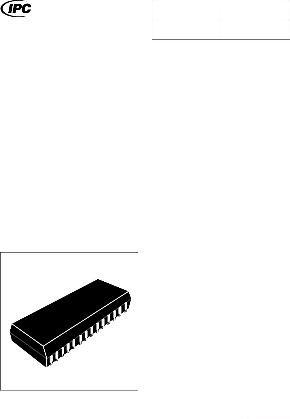
1.0 SCOPE
This subsection provides the component and land pattern
dimensions for small outline integrated circuits with ‘‘J’’ leads
(SOJ components). Basic construction of the SOJ device is
also covered. At the end of this subsection is a listing of the
tolerances and target solder joint dimensions used to arrive at
the land pattern dimensions.
2.0 APPLICABLE DOCUMENTS
See Section 10.0 for documents applicable to the subsec-
tions.
3.0 COMPONENT DESCRIPTIONS
The two-sided J lead family is a small outline family identified
by the dimension of the body size in inches. For example, the
SOJ/300 has a body size of 0.300 inches or 7.63 mm, the
SOJ/350 has a body size of 0.350 inches or 8.88 mm, the
SOJ/400 has a body size of 0.400 inches or 10.12 mm, and
the SOJ/450 has a body size of 0.450 inches or 11.38 mm.
Package lead counts range from 14 to 28 pins.
The small-outline ‘‘J’’ (SOJ) package has leads on two sides,
similar to a DIP. The lead configuration, like the letter J,
extends out the side of the package and bends under the
package forming a J bend. The point of contact of the lead to
the land
pattern is at the apex of the J bend and is the basis for the
span of the land pattern.
The leads must be coplanar within 0.1 mm. That is, when the
component is placed on a flat surface, no lead may be more
than 0.1 mm off the flat surface.
The SOJ package takes advantage of chips having parallel
address or data line layouts. For example, memory IC’s are
often used in multiples, and buss lines connect to the same
pin on each chip. Memory chips in SOJ packages can be
placed close to one another because of the parallel pin layout
and the use of ‘‘J’’ leads. With high capacity memory sys-
tems, the space savings can be significant.
3.1 Basic Construction
See Figure 1. Basic construction
consists of a plastic body, and metallic ‘‘J’’ leads.
3.1.1 Termination Materials
Leads must be solder-
coated with a tin/lead alloy. The solder should contain
between 58 to 68% lead. Solder may be applied to theleads
by hot dipping or by plating from solution. Plated solder termi-
nations should be subjected to post-plating reflow operation
to fuse the solder. The tin/lead finishshould be at least 0l.0075
mm [0.0003 in] thick.
3.1.2 Marking
The SOIC family of parts is generally
marked with manufacturers part numbers, manufacturers
name or symbol, and a pin 1 indicator. Some parts may have
a pin 1 feature in the case shape instead of pin 1 marking.
Additional markings may include date code/manufacturing lot
and/or manufacturing location.
3.1.3 Carrier Package Format
Components may be pro-
vided in tube or tape packaging. Tape is preferred for best
handling and high volume applications. Bulk packaging is not
acceptable because of lead coplanarity requirements required
for placement and soldering. EIA-481 provides details on tape
requirements.
3.1.4 Process Considerations
J lead packages are nor-
mally processed using standard solder reflow processes.
Parts should be capable of withstanding ten cycles through a
standard reflow system operating at 215°C. Each cycle shall
consist of 60 seconds exposure at 215°C.
IPC-782-10-1-1
Figure 1 SOJ construction
IPC-SM-782
Surface Mount Design
and Land Pattern Standard
Date
5/96
Section
10.1
Revision
A
Subject
SOJ
Page1of6
电子技术应用 www.ChinaAET.com
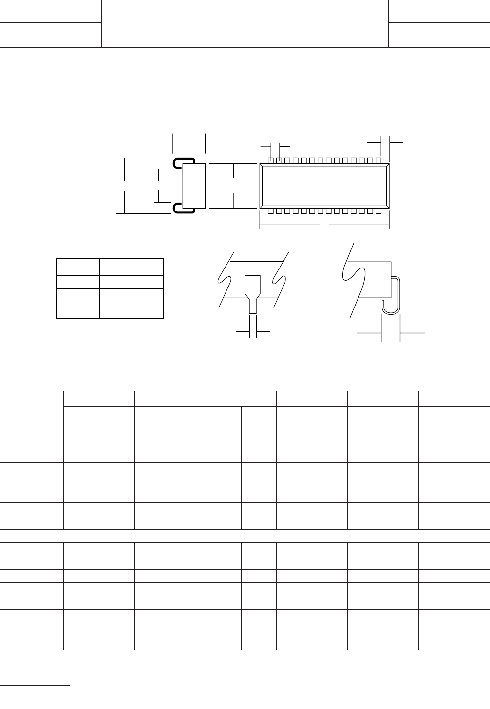
4.0 COMPONENT DIMENSIONS
In this subsection, Figures 2a–2b provide the component
dimensions for SOJ components. (Also see page 4.)
Component
Identifier (Pin
Count)
L (mm) S (mm) W (mm) T (mm) B (mm) H (mm) P (mm)
min max min max min max min max m in max max basic
SOJ 14/300 8.38 8.76 4.38 5.06 0.38 0.51 1.60 2.00 9.65 9.96 3.75 1.27
SOJ 16/300 8.38 8.76 4.38 5.06 0.38 0.51 1.60 2.00 10.92 11.23 3.75 1.27
SOJ 18/300 8.38 8.76 4.38 5.06 0.38 0.51 1.60 2.00 12.19 12 .50 3.75 1.27
SOJ 20/300 8.38 8.76 4.38 5.06 0.38 0.51 1.60 2.00 13.46 13.77 3.75 1.27
SOJ 22/300 8.38 8.76 4.38 5.06 0.38 0.51 1.60 2.00 14.73 15.04 3.75 1.27
SOJ 24/300 8.38 8.76 4.38 5.06 0.38 0.51 1.60 2.00 16.00 16.31 3.75 1.27
SOJ 26/300 8.38 8.76 4.38 5.06 0.38 0.51 1.60 2.00 17.27 17.58 3.75 1.27
SOJ 28/300 8.38 8.76 4.38 5.06 0.38 0.51 1.60 2.00 18.54 18.85 3.75 1.27
SOJ 14/350 9.65 10.03 5.65 6.33 0.38 0.51 1.60 2.00 9.65 9.96 3.75 1.27
SOJ 16/350 9.65 10.03 5.65 6.33 0.38 0.51 1.60 2.00 10.92 11.23 3.75 1.27
SOJ 18/350 9.65 10.03 5.65 6.33 0.38 0.51 1.60 2.00 12.19 12.50 3.75 1.27
SOJ 20/350 9.65 10.03 5.65 6.33 0.38 0.51 1.60 2.00 13.46 13.77 3.75 1.27
SOJ 22/350 9.65 10.03 5.65 6.33 0.38 0.51 1.60 2.00 14.73 15.04 3.75 1.27
SOJ 24/350 9.65 10.03 5.65 6.33 0.38 0.51 1.60 2.00 16.00 16.31 3.75 1.27
SOJ 26/350 9.65 10.03 5.65 6.33 0.38 0.51 1.60 2.00 17.27 17.58 3.75 1.27
SOJ 28/350 9.65 10.03 5.65 6.33 0.38 0.51 1.60 2.00 18.54 18.85 3.75 1.27
Figure 2a SOJ component dimensions
▼
▼
▼
▼
▼
▼
▼
P
B
1.02
1.17
A
▼
SL
▼
▼
▼
▼
▼
▼
H
▼
▼
T
▼
▼
W
A (in.)
ref.
0.300
0.350
A (mm)
min max
7.49 7.75
8.76 9.02
IPC-782-101-2a
IPC-SM-782
Subject
SOJ
Date
5/96
Section
10.1
Revision
A
Page2of6
电子技术应用 www.ChinaAET.com