IPC-SM-782A 表面安装设计和焊盘设计标准(带BGA).pdf - 第146页
Page Intentionally Left Blank IPC-SM-782 Subject Components with Gullwing Leads on Four Sides Date 8/93 Section 11.0 Revision P a g e2o f2 电子技术应用 www.ChinaAET.com
1.0 INTRODUCTION
This section covers land patterns for components with gull-
wing leads on four sides. Each subsection contains informa-
tion in accordance with the following format:
1.0 Scope
2.0 Applicable Documents
3.0 General Component Description (Figure 1)
4.0 Component Dimensions (Figure 2)
5.0 Land Pattern Dimensions (Figure 3)
6.0 Tolerance and Solder Joint Analysis (Figure 4)
The following is the table of contents for this section:
2.0 APPLICABLE DOCUMENTS
The following documents, of the issue in effect on the revision
date of this section, form a part of this specification to the
extent specified herein.
2.1 Electronic Industries Association (EIA)
1
EIA-481-A
Taping of Surface Mount Components for Auto-
matic Placement
EIA-481-3
32 mm, 44 mm, and 56 mm Embossed Carrier
Taping of Surface Mount Components for Automated Han-
dling
JEDEC Publication 95
Registered and Standard Outlines for
Solid State and Related Products:
MO 108, issue ‘‘A,’’ dated 10/90
MO 112, issue ‘‘A,’’ dated 8/90
MO 136, issue ‘‘A,’’ dated 8/92, now MS-026
MO 143, issue ‘‘A,’’ dated 3/93, now MS-029
2.2 Electronic Industries Association of Japan (EIAJ)
EIAJ-ED-7404
General Rules for the Preparation of Outline
Drawings of Integrated Circuits
2.3 International Electrotechnical Commission (IEC)
2
IEC 97
Grid Elements
3.0 General Information
3.1 General Component Description
The four-sided gull
wing family is characterized by gull wing leads on four sides of
a square or rectangular package. The family includes both
molded plastic and ceramic case styles. The acronyms PQFP,
Plastic Quad Flat Pack and CQFP, Ceramic Quad Flat Pack,
are also used to describe the family.
There are several lead pitches within the family from 1.0 mm
to 0.30 mm. High lead-count packages are available in this
family that accommodate complex, high lead-count chips.
3.2 Marking
The PFQP and CQFP families of parts are
generally marked with manufacturers part numbers, manufac-
turers name or symbol, and a pin 1 indicator. Some parts may
have a pin 1 feature in the case shape instead of pin 1 mark-
ing. Additional markings may include date code/
manufacturing lot and/or manufacturing location.
3.3 Carrier Package Format
Components may be pro-
vided in tube but packaging tray carriers are preferred for best
handling and high volume applications. Bulk packaging is not
acceptable because of lead coplanarity required for place-
ment and soldering.
3.3 Process Considerations
PQFP and CQFP packages
are normally processed by solder reflow operations.
High lead-count fine pitch parts may require special process-
ing outside the normal pick/place and reflow manufacturing
operations.
Separate pick/place, excise, and reflow processes are some-
times used as an alternate to normal SMT processes.
1. Application for copies should be addressed to Global Engi-
neering Documents, 1990 M St. N.W., Washington, DC
20036.
2. Application for copies should be addressed to IEC, 3 rue
de Varembe, PO Box 131 - 1211 Geneva 20, Switzerland
IPC-SM-782
Surface Mount Design
and Land Pattern Standard
Date
8/93
Section
11.0
Revision Subject
Components with
Gullwing Leads on Four
Sides
Page1of2
电子技术应用 www.ChinaAET.com

Page Intentionally Left Blank
IPC-SM-782
Subject
Components with Gullwing Leads on Four Sides
Date
8/93
Section
11.0
Revision
Page2of2
电子技术应用 www.ChinaAET.com
1.0 SCOPE
This subsection provides the component and land pattern
dimensions for PQFP (Plastic Quad Flat Pack) components.
Basic construction of the PQFP device is also covered. At the
end of this subsection is a listing of the tolerances and target
solder joint dimensions used to arrive at the land pattern
dimensions.
2.0 APPLICABLE DOCUMENTS
See Section 11.0 and the following for documents applicable
to the subsections.
Electronic Industries Association (EIA)
JEDEC Publication 95
Registered and Standard Outlines for
Solid State and Related Products, ‘‘Low Profile Plastic Quad
Flat Pack Family 0.025 Lead Spacing (Gullwing), Outline
MO-086, issue ‘‘B,’’ dated 6/90
Application for copies should be addressed to:
Global Engineering Documents
1990 M Street N.W.
Washington, DC
3.0 COMPONENT DESCRIPTIONS
Flatpacks are widely used in a variety of applications for com-
mercial, industrial, or military electronics.
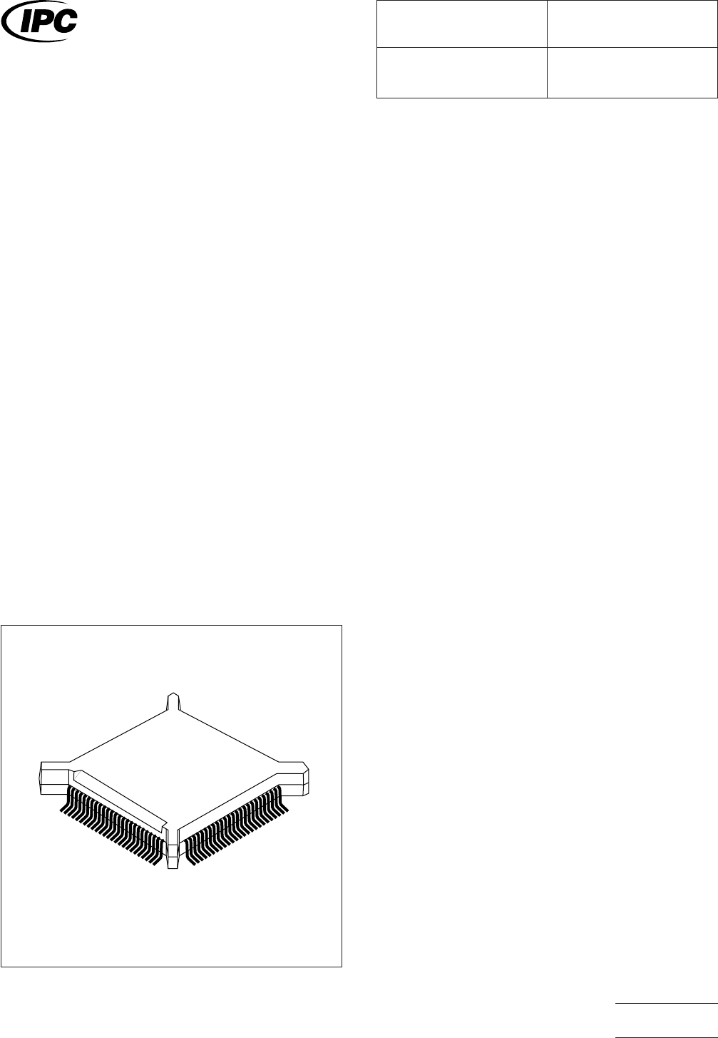
3.1 Basic Construction
See Figure 1. PQFPs have leads
on a 0.635 mm pitch.
3.1.1 Termination Materials
Leads must be solder-
coated with a tin/lead alloy. The solder should contain
between 58 to 68% tin. Solder may be applied to the leads by
hot dipping or by plating from solution. Plated solder termina-
tions should be subjected to post-plating reflow operation to
fuse the solder. The tin/lead finish should be at least 0.0075
mm [0.0003 in] thick.
3.1.2 Marking
All parts shall be marked with a part number
and an index area. The index area shall identify the location of
pin 1.
3.1.3 Carrier Package Format
The carrier package for-
mat for PFQPs is the tube format; however, packaging trays
provide the best handling capability.
3.1.4 Process Considerations
PQFPs are usually pro-
cessed using standard solder reflow processes. Parts should
be capable of withstanding ten cycles through a standard
reflow system operating at 215°C. Each cycle shall consist of
60 seconds exposure at 215°C.
IPC-782-11-1-1
Figure 1 PQFP construction
IPC-SM-782
Surface Mount Design
and Land Pattern Standard
Date
5/96
Section
11.1
Revision
A
Subject
PQFP
Page1of4
电子技术应用 www.ChinaAET.com