IPC-SM-782A 表面安装设计和焊盘设计标准(带BGA).pdf - 第147页
1.0 SCOPE This subsection provides the component and land pattern dimensions for PQFP (Plastic Quad Flat Pack) components. Basic construction of the PQFP device is also covered. At the end of this subsection is a listing…

Page Intentionally Left Blank
IPC-SM-782
Subject
Components with Gullwing Leads on Four Sides
Date
8/93
Section
11.0
Revision
Page2of2
电子技术应用 www.ChinaAET.com
1.0 SCOPE
This subsection provides the component and land pattern
dimensions for PQFP (Plastic Quad Flat Pack) components.
Basic construction of the PQFP device is also covered. At the
end of this subsection is a listing of the tolerances and target
solder joint dimensions used to arrive at the land pattern
dimensions.
2.0 APPLICABLE DOCUMENTS
See Section 11.0 and the following for documents applicable
to the subsections.
Electronic Industries Association (EIA)
JEDEC Publication 95
Registered and Standard Outlines for
Solid State and Related Products, ‘‘Low Profile Plastic Quad
Flat Pack Family 0.025 Lead Spacing (Gullwing), Outline
MO-086, issue ‘‘B,’’ dated 6/90
Application for copies should be addressed to:
Global Engineering Documents
1990 M Street N.W.
Washington, DC
3.0 COMPONENT DESCRIPTIONS
Flatpacks are widely used in a variety of applications for com-
mercial, industrial, or military electronics.
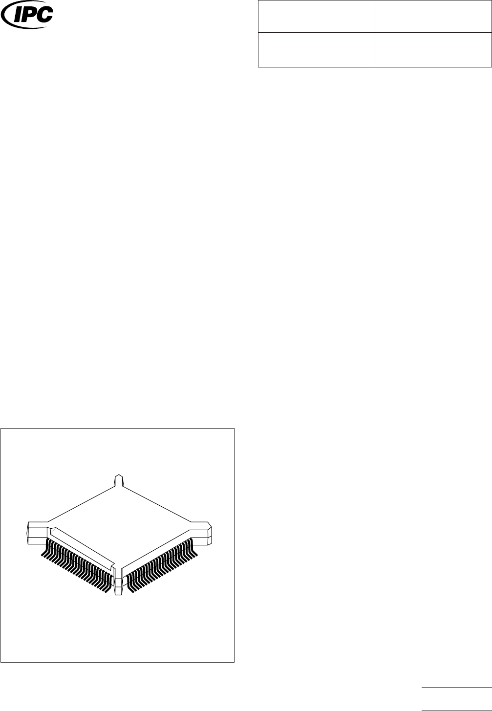
3.1 Basic Construction
See Figure 1. PQFPs have leads
on a 0.635 mm pitch.
3.1.1 Termination Materials
Leads must be solder-
coated with a tin/lead alloy. The solder should contain
between 58 to 68% tin. Solder may be applied to the leads by
hot dipping or by plating from solution. Plated solder termina-
tions should be subjected to post-plating reflow operation to
fuse the solder. The tin/lead finish should be at least 0.0075
mm [0.0003 in] thick.
3.1.2 Marking
All parts shall be marked with a part number
and an index area. The index area shall identify the location of
pin 1.
3.1.3 Carrier Package Format
The carrier package for-
mat for PFQPs is the tube format; however, packaging trays
provide the best handling capability.
3.1.4 Process Considerations
PQFPs are usually pro-
cessed using standard solder reflow processes. Parts should
be capable of withstanding ten cycles through a standard
reflow system operating at 215°C. Each cycle shall consist of
60 seconds exposure at 215°C.
IPC-782-11-1-1
Figure 1 PQFP construction
IPC-SM-782
Surface Mount Design
and Land Pattern Standard
Date
5/96
Section
11.1
Revision
A
Subject
PQFP
Page1of4
电子技术应用 www.ChinaAET.com
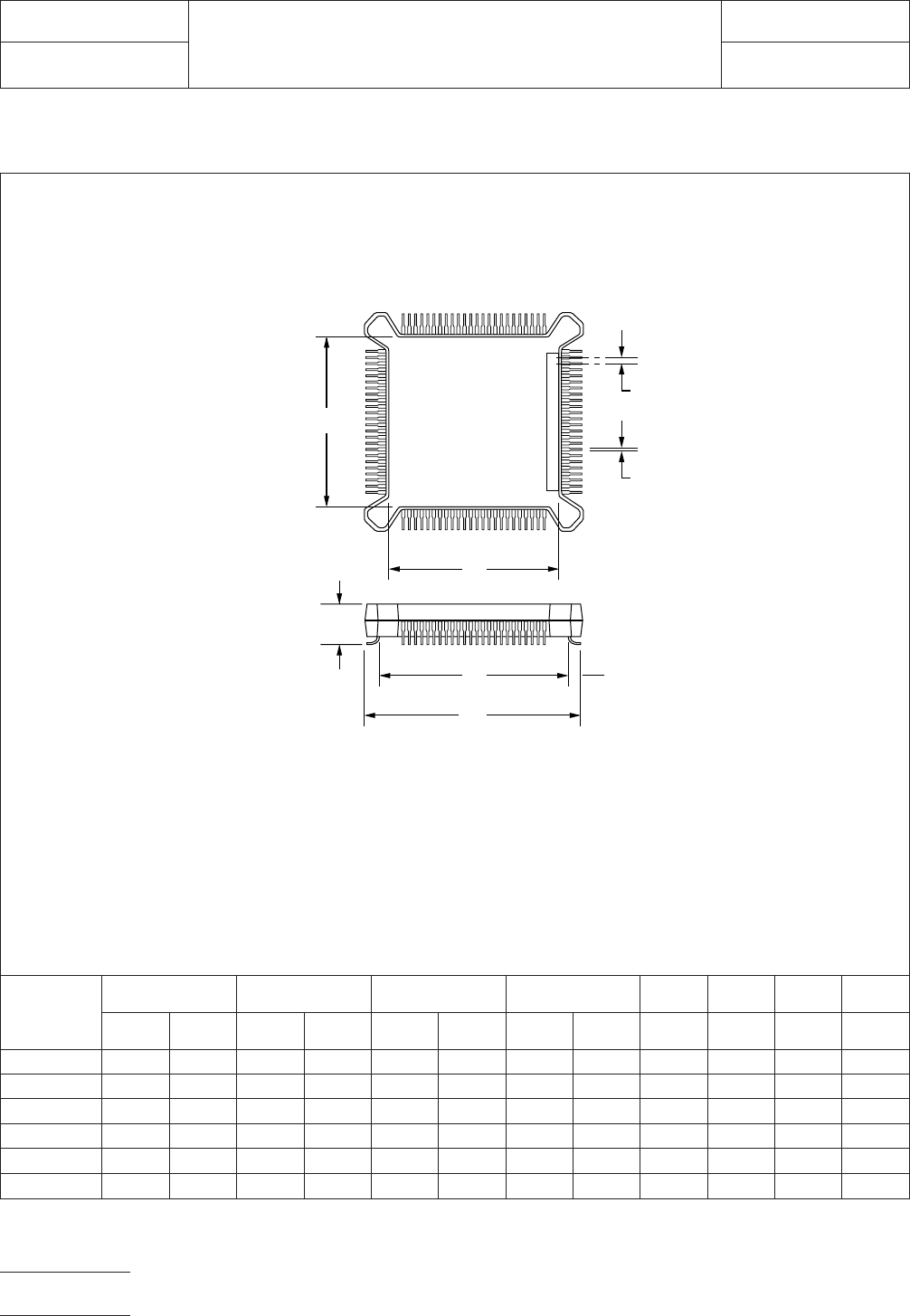
4.0 COMPONENT DIMENSIONS
Figure 2 provides the component dimensions for PQFP components.
PQFP
Component
Identifier
(Pin Count)
L (mm) S (mm) W (mm) T (mm) A (mm) B (mm) E (mm) H (mm)
min max min max min max min max max max basic max
PQFP 84 19.55 20.05 17.55 18.16 0.20 0.30 0.75 1.00 16.80 16.80 0.635 4.57
PQFP 100 22.10 22.60 20.10 20.71 0.20 0.30 0.75 1.00 19.35 19.35 0.635 4.57
PQFP 132 27.20 27.70 25.25 25.81 0.20 0.30 0.75 1.00 24.40 24.40 0.635 4.57
PQFP 164 32.25 32.75 30.25 30.86 0.20 0.30 0.75 1.00 29.40 29.40 0.635 4.75
PQFP 196 37.35 37.85 35.35 35.96 0.20 0.30 0.75 1.00 34.40 34.40 0.635 4.57
PQFP 244 41.65 42.15 39.65 40.26 0.20 0.30 0.75 1.00 45.40 45.40 0.635 4.57
Figure 2 PQFP dimensions
S
L
H
T
W
E
A
B
IPC-782-11-1-2
IPC-SM-782
Subject
PQFP
Date
5/96
Section
11.1
Revision
A
Page2of4
电子技术应用 www.ChinaAET.com