IPC-SM-782A 表面安装设计和焊盘设计标准(带BGA).pdf - 第150页
6.0 TOLERANCE AND SOLDER JOINT ANALYSIS Figure 4 provides an analysis of tolerance assumptions and resultant solder joints based on the land pattern dimensions shown in Figure 3. Tolerances for the component dimensions, …
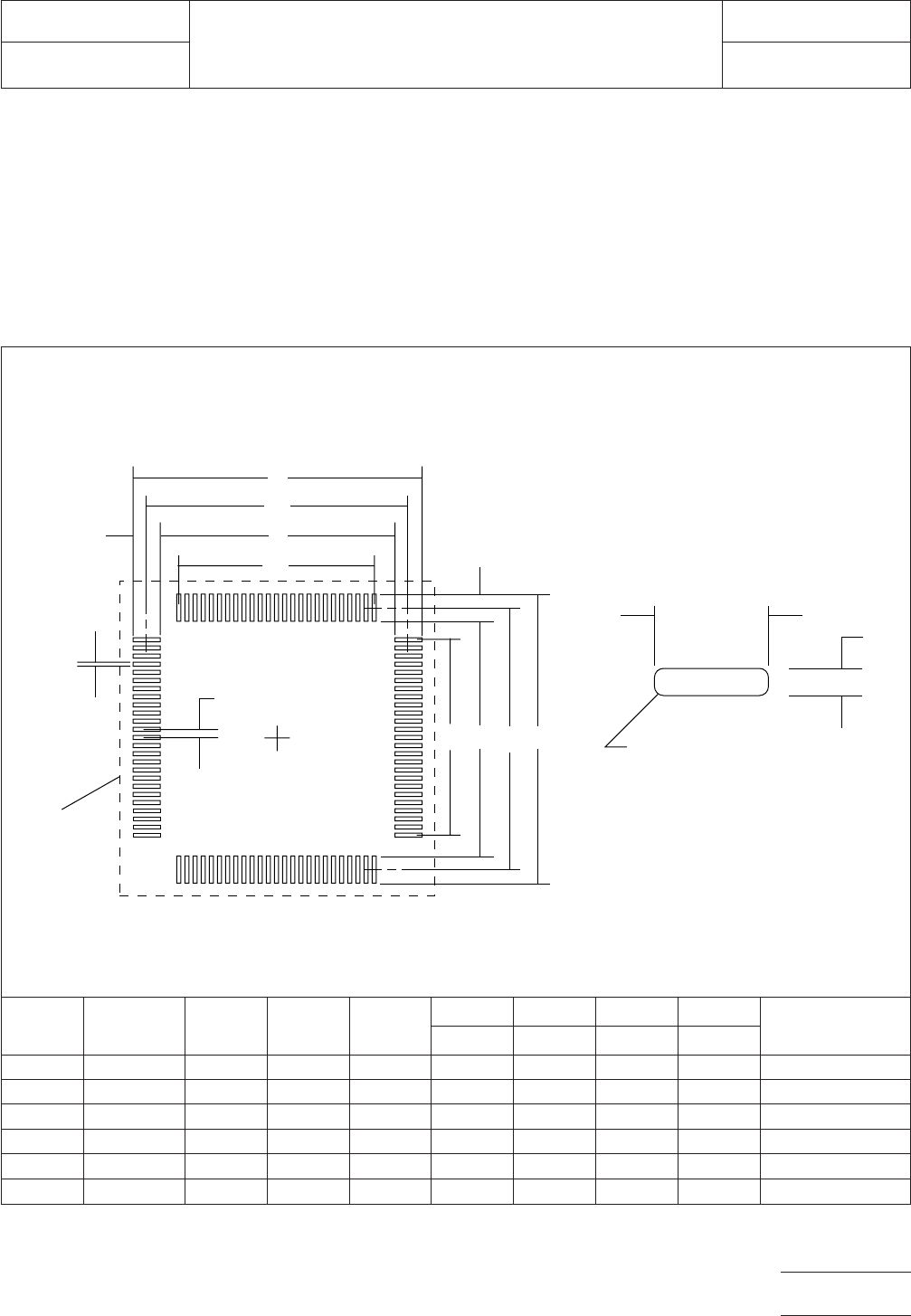
5.0 LAND PATTERN DIMENSIONS
Figure 3 provides the land pattern dimensions for PQFP com-
ponents. These numbers represent industry consensus on the
best dimensions based on empirical knowledge of fabricated
land patterns.
In the table, the dimensions shown are at maximum material
condition (MMC). The least material condition (LMC) should
not exceed the fabrication (F) allowance shown on page 4.
The LMC and the MMC provide the limits for each dimension.
The dotted line in Figure 3 shows the grid placement court-
yard which is the area required to place land patterns and
their respective components in adjacent proximity without
interference or shorting. Numbers in the table represent the
number of grid elements (each element is 0.5 by 0.5 mm) in
accordance with the international grid detailed in IEC publica-
tion 97.
RLP No.
Component
Identifier
(Pin Count) Z (mm) G (mm) X (mm)
Y (mm) C (mm) D (mm) E (mm)
Placement Grid
(No. of Grid
Elements)
ref ref ref basic
530A PQFP 84 20.60 17.00 0.35 1.80 18.80 12.70 0.63 44X44
531A PQFP 100 23.20 19.60 0.35 1.80 21.40 15.24 0.63 50X50
532A PQFP 132 28.20 24.60 0.35 1.80 26.40 20.32 0.63 58X58
533A PQFP 164 33.40 29.80 0.35 1.80 31.60 25.40 0.63 68X68
534A PQFP 196 38.40 34.80 0.35 1.80 36.60 30.48 0.63 80X80
535A PQFP 244 42.80 39.20 0.35 1.80 41.00 38.10 0.63 88X88
Figure 3
E
▼
▼
▼
▼
X
Y
Z
G
D
▼
▼
▼
▼
▼
Y
X
Full radius optional
▼
▼
▼
▼
▼
Grid
placement
courtyard
▼
▼
▼
C
▼
▼
▼
▼
▼
▼
▼
▼
▼
▼
▼
Y
DGCZ
IPC-782-11-1-3
IPC-SM-782
Subject
PQFP
Date
5/96
Section
11.1
Revision
A
Page3of4
电子技术应用 www.ChinaAET.com
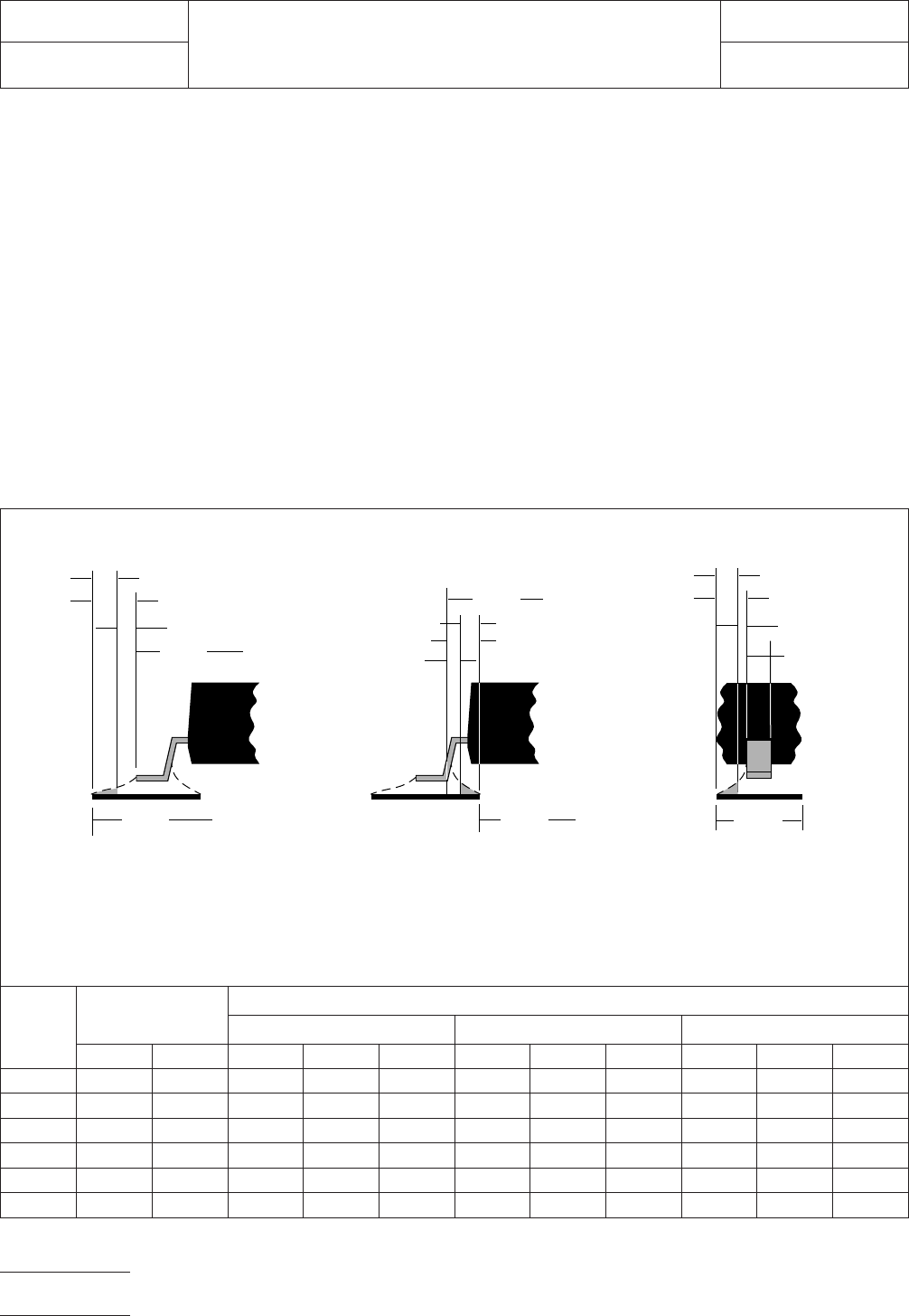
6.0 TOLERANCE AND SOLDER JOINT ANALYSIS
Figure 4 provides an analysis of tolerance assumptions and
resultant solder joints based on the land pattern dimensions
shown in Figure 3. Tolerances for the component dimensions,
the land pattern dimensions (fabrication tolerances on the
interconnecting substrate), and the component placement
equipment accuracy are all taken into consideration.
Figure 4 provides the solder joint minimums for toe, heel, and
side fillets, as discussed in Section 3.3. The tolerances are
addressed in a statistical mode, and assume even distribution
of the tolerances for component, fabrication, and placement
accuracy.
Individual tolerances for fabrication (‘‘F’’) and component
placement equipment accuracy (‘‘P’’) are assumed to be as
given in the table. These numbers may be modified based on
user equipment capability or fabrication criteria. Component
tolerance ranges (C
L
,C
S
, and C
W
) are derived by subtracting
minimum from maximum dimensions given in Figure 2. The
user may also modify these numbers, based on experience
with their suppliers. Modification of tolerances may result in
alternate land patterns (patterns with dimensions other than
the IPC registered land pattern dimensions).
The dimensions for minimum solder fillets at the toe, heel, or
side (J
T
,J
H
,J
S
) have been determined based on industry
empirical knowledge and reliability testing. Solder joint
strength is greatly determined by solder volume. An observ-
able solder fillet is necessary for evidence of proper wetting.
Thus, the values in the table usually provide for a positive sol-
der fillet. Nevertheless, the user may increase or decrease the
minimum value based on process capability.
RLP No.
Tolerance
Asssumptions
(mm)
Solder Joint
Toe (mm) Heel (mm) Side (mm)
FPC
L
J
T
min J
T
max C
S
J
H
min J
H
max C
W
J
S
min J
S
max
530A 0.10 0.10 0.50 0.27 0.53 0.61 0.27 0.58 0.10 -0.01 0.08
531A 0.10 0.10 0.50 0.29 0.55 0.61 0.24 0.56 0.10 -0.01 0.08
532A 0.10 0.10 0.50 0.24 0.50 0.61 0.29 0.61 0.10 -0.01 0.08
533A 0.10 0.10 0.50 0.32 0.58 0.61 0.22 0.53 0.10 -0.01 0.08
534A 0.10 0.10 0.50 0.27 0.53 0.61 0.27 0.58 0.10 -0.01 0.08
535A 0.10 0.10 0.50 0.32 0.57 0.61 0.22 0.53 0.10 -0.01 0.08
Figure 4 Tolerance and solder joint analysis
Zmax
Lmin
▼
▼
▼
▼
1
/2 T
T
J
T
min
Zmax = Lmin + 2J
T
min + T
T
Where:
J
T
min = Minimum toe fillet
T
T
= Combined tolerances
at toe fillet
Smax
J
H
min
Gmin = Smax - 2J
H
min - T
H
Where:
J
H
min = Minimum heel fillet
T
H
= Combined tolerances
at heel fillet
1
/2 T
H
Xmax
Xmax = Wmin + 2J
S
min + T
S
Where:
J
S
min = Minimum side fillet
T
S
= Combined tolerances
at side fillet
▼
▼
Toe Fillet
▼
▼
▼
Heel Fillet Side Fillet
▼
▼
▼
▼
▼
J
T
max
J
H
max
J
S
min
▼
▼
▼
▼
▼
▼
▼
▼
▼
▼
▼
▼
▼
▼
▼
Gmin
▼
1
/2 T
S
J
S
max
▼
▼
▼
Wmin
▼
IPC-782-11-1-4
IPC-SM-782
Subject
PQFP
Date
5/96
Section
11.1
Revision
A
Page4of4
电子技术应用 www.ChinaAET.com
1.0 SCOPE
This subsection provides the component and land pattern
dimensions for square SQFP (Shrink Quad Flat Pack) and QFP
(metric plastic quad flat pack) components. Basic construc-
tion of the SQFP device is also covered. At the end of this
subsection is a listing of the tolerances and target solder joint
dimensions used to arrive at the land pattern dimensions.
2.0 APPLICABLE DOCUMENTS
See Section 11.0 and the following for documents applicable
to this subsection.
2.1 Electronic Industries Association (EIA)
JEDEC Publication 95
Registered and Standard Outlines for
Solid State and Related Products, ‘‘Metric Quad Flat Pack
Family 3.2 mm Footprint,’’ Outline MO-108, issue ‘‘A,’’ dated
10/90
Application for copies should be addressed to:
Global Engineering Documents
1990 M Street N.W.
Washington, DC
2.2 Electronic Industries Association of Japan (EIAJ)
EIAJ-ED-7404-1
General Rules for the Preparation of Outline
Drawings of Integrated Circuits Fine Pitch Quad Flat Packages
(dated January 26, 1989)
3.0 COMPONENT DESCRIPTIONS
Flatpacks are widely used in a variety of applications for com-
mercial, industrial, or military electronics.
3.1 Basic Construction
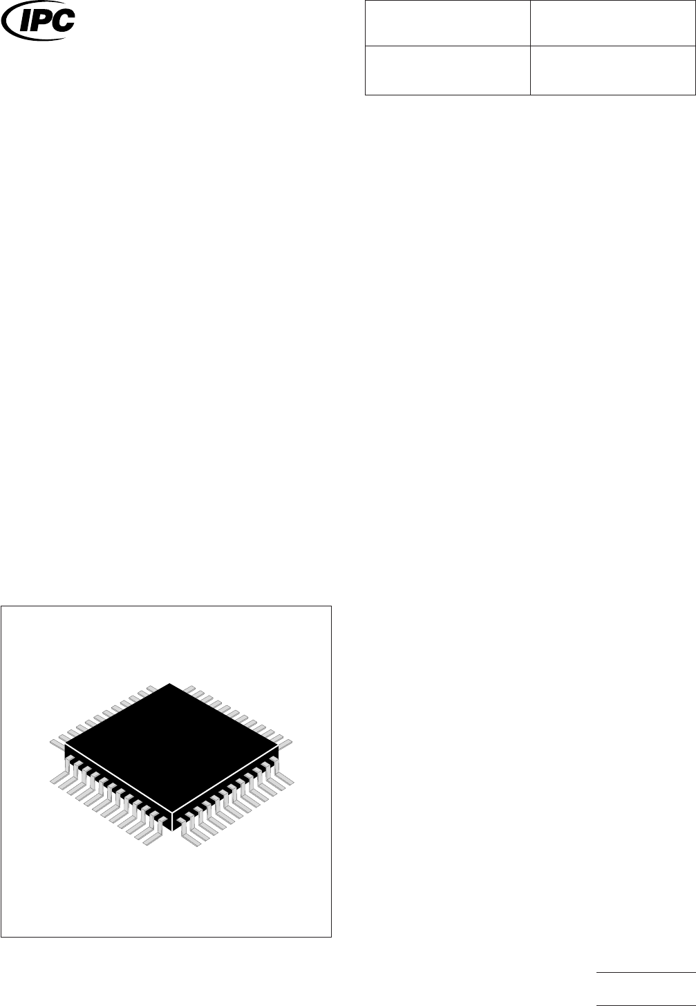
See Figure 1.
The shrink quad flat pack has been developed for applications
requiring low height and high density. The SQFP, along with
the TSOP components, are frequently used in memory card
applications. The square SQFP family comes in 13 standard
sizes, each of which sizes can come in either a 0.5, 0.4, or 0.3
mm pitch. There are therefore 39 configurations for square
SQFPs.
Two different pin counts are allowed for each package and
the component will still meet the standard (e.g., a 5x5 pack-
age with a 0.3 mm pitch can have either 56 or 48 pins, and
still meet EIAJ-7404-1).
QFPs are also square and come in larger pitches. Wherever
applicable, the body sizes of the components identified in Fig-
ures 2 and 3 show the relationships and pin numbers for
SQFPs and QFPs that have the same body size.
3.1.1 Termination Materials
Leads must be solder-
coated with a tin/lead alloy. The solder should contain
between 58 to 68% tin. Solder may be applied to the leads by
hot dipping or by plating from solution. Plated solder termina-
tions should be subjected to post-plating reflow operation to
fuse the solder. The tin/lead finish should be at least 0.0075
mm [0.0003 in] thick.
3.1.2 Marking
All parts shall be marked with a part number
and an index area. The index area shall identify the location of
pin 1.
3.1.3 Carrier Package Format
The carrier package for-
mat for flatpacks may be tube format; but, in most instances,
flatpacks are delivered in a carrier tray.
3.1.4 Process Considerations
SQFPs and QFPs are usu-
ally processed using standard solder reflow processes. Parts
should be capable of withstanding ten cycles through a stan-
dard reflow system operating at 215°C. Each cycle shall con-
sist of 60 seconds exposure and 215°C.
IPC-782-11-2-1
Figure 1 SQFP & QFP (Square)
IPC-SM-782
Surface Mount Design
and Land Pattern Standard
Date
5/96
Section
11.2
Revision
A
Subject
SQFP/QFP (Square)
Page1of10
电子技术应用 www.ChinaAET.com