IPC-SM-782A 表面安装设计和焊盘设计标准(带BGA).pdf - 第174页
4.0 COMPONENT DIMENSIONS Figure 2 provides the component dimensions for PLCC (Square) components. Component Identifier L (mm) S (mm) W (mm) T (mm) A (mm) B (mm) J (mm) H (mm) P (mm) min max min max min max min max min max…
1.0 SCOPE
This subsection provides the component and land pattern
dimensions for plastic leaded chip carriers, square (PLCC
components) with J leads on four sides. Basic construction of
the PLCC device is also covered. At the end of this subsec-
tion is a listing of the tolerances and target solder joint dimen-
sions used to arrive at the land pattern dimensions.
2.0 APPLICABLE DOCUMENTS
See Section 12.0 for documents applicable
to the subsections.
2.1 Electronic Industries Association (EIA)
JEDEC Publication 95
Registered and Standard Outlines for
Solid State and Related Products, ‘‘Plastic Chip Carrier
(PLCC) Family, 1.27 mm [0.050 in] Lead Spacing, Square,’’
Outline MO-047, issue ‘‘B,’’ dated 11/88
Application for copies should be addressed to:
Global Engineering Documents
1990 M Street N.W.
Washington, DC
3.0 COMPONENT DESCRIPTIONS
Plastic leaded chip carriers are employed where a hermetic
seal is not required. Other constraints include limited tempera-
ture range (typically 0°C or 70°C) and nominal environmental
protection. As with plastic DIPs, they have the advantage of
low cost as compared to ceramic packages.
3.1.1 Pre-molded Plastic Chip Carriers
The pre-molded
plastic chip carrier was designed to be connected to the P&I
substrate by means of a socket. Spring pressure on both
sides of the package is intended to constrain movement as
well as allow for substrate warpage as high as 0.5%. Solder
attach to the P&I substrate is also possible. The design is also
intended to make use of silicone encapsulant technology for
chip coverage and protection.
3.1.2 Post-molded Plastic Chip Carriers
The post-
molded plastic leaded chip carrier is composed of a compos-
ite metal/dielectric assembly that includes a conductor lead
frame and a molded insulating body. Compared to the pre-
molded package which has an aperture for mounting micro-
electronic components, the post-molded package comes
complete with no apertures. In both types of plastic chip car-
riers, all necessary plating operations are performed by the
package manufacturer to eliminate tinning or plating by the
user.
The Joint Device Engineering Council (JEDEC) defines the
Type A Leaded Chip Carrier as a plastic package with leads
wrapped down and around the body on all four sides. This
package can be either directly mounted to a printed wiring
board or used with a socket. It is available with 28, 44, 52, 68,
84, 100, or 124 leads. This family is based on 1.27 mm [0.050
in] lead pitch. The original mechanical outline drawing of this
package was defined based on a premolded package. How-
ever, actual construction is not specified and the package
could be of post-molded construction.
Post-molded packages which have J-lead configuration and
are
JEDC standard MO-047, are available in 20-, 28-, 44-, 52-,
68-, 84-, 100- and 124-lead counts with the
same spacing.
3.1.3 Marking
All parts shall be marked with a part number
and ‘‘Pin 1’’ location. ‘‘Pin 1’’ location may be molded into the
plastic body.
3.1.4 Carrier Package Format
Bulk rods, 24 mm tape/
8–12 mm pitch is preferred for best handling. Tube carriers
are also used.
3.1.5 Resistance to Soldering
Parts should be capable of
withstanding ten cycles through a standard reflow system
operating at 215°C. Each cycle shall consist of 60 seconds
exposure at 215°C. Parts must also be capable of withstand-
ing a minimum of 10 seconds immersion in molten solder at
260°C.
IPC-782-12-1-1
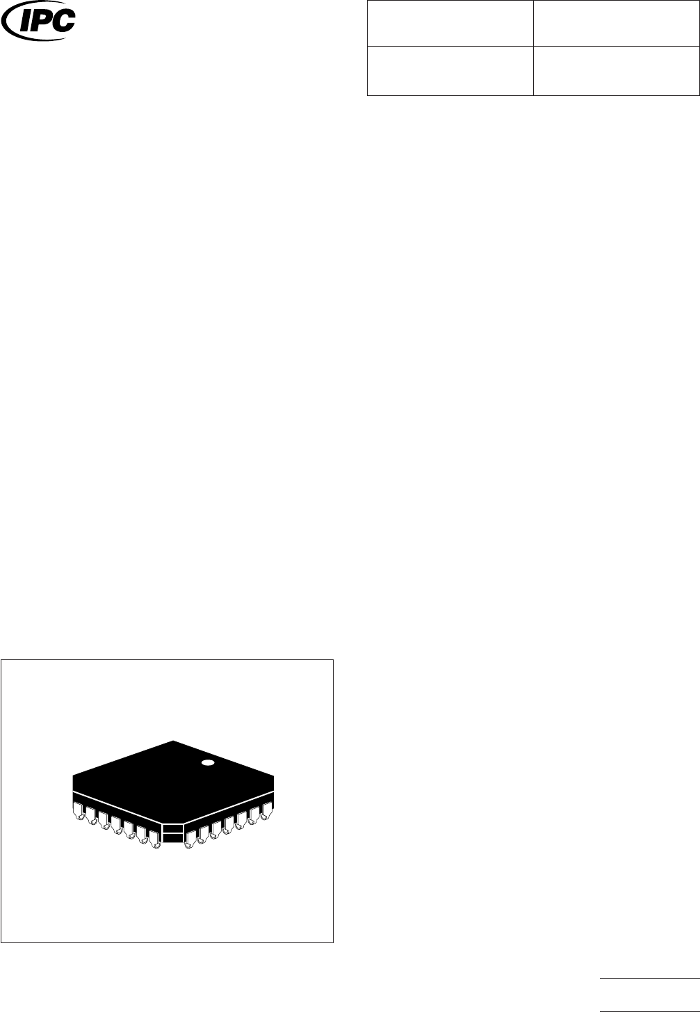
Figure 1 PLCC (Square)
IPC-SM-782
Surface Mount Design
and Land Pattern Standard
Date
5/96
Section
12.1
Revision
A
Subject
PLCC (Square)
Page1of4
电子技术应用 www.ChinaAET.com
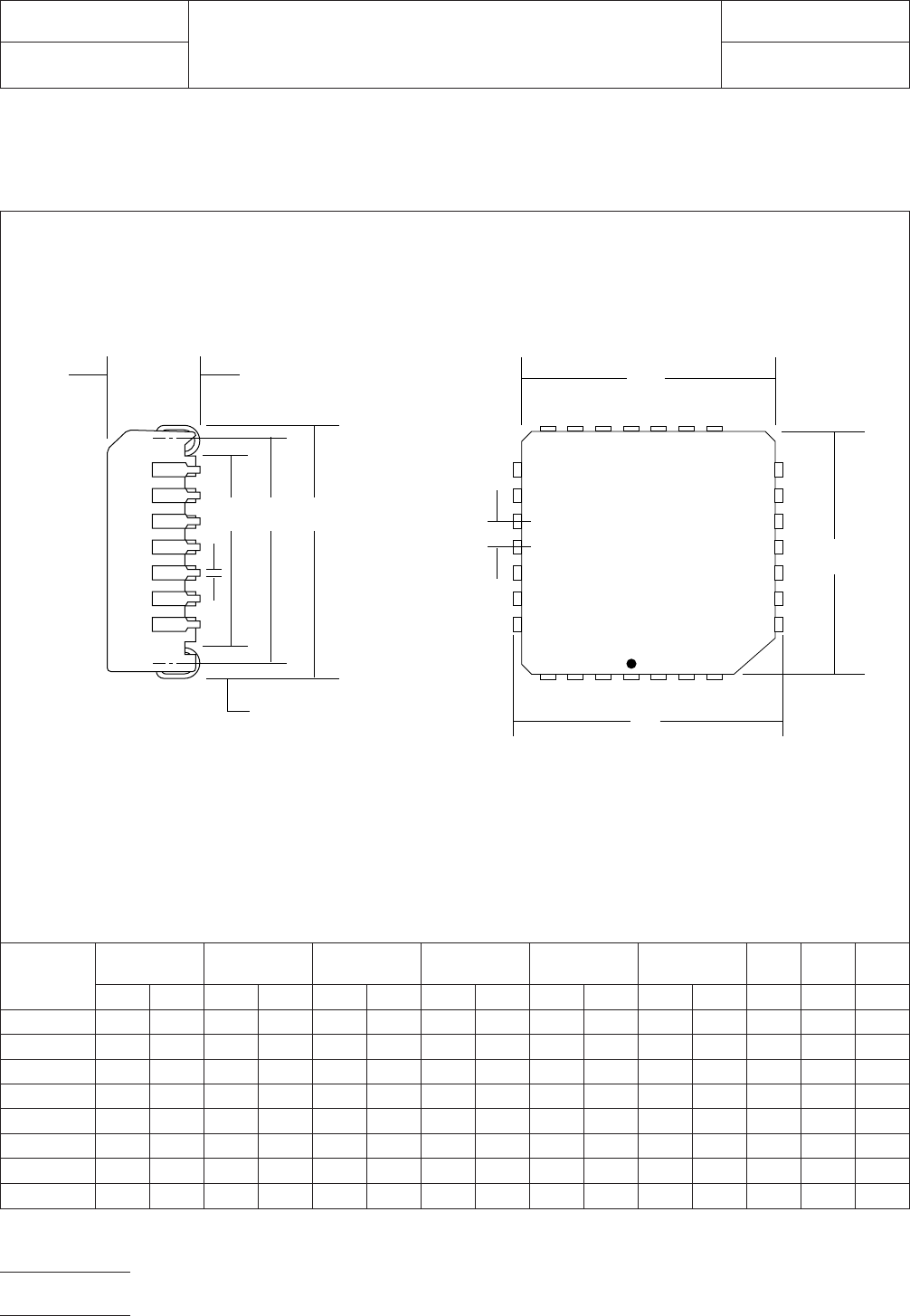
4.0 COMPONENT DIMENSIONS
Figure 2 provides the component dimensions for PLCC
(Square) components.
Component
Identifier
L (mm) S (mm) W (mm) T (mm) A (mm) B (mm)
J
(mm)
H
(mm)
P
(mm)
min max min max min max min max min max min max ref max basic
PLCC-20 9.78 10.03 5.78 6.53 0.33 0.53 1.50 2.00 8.89 9.04 8.89 9.04 7.87 4.57 1.27
PLCC-28 12.32 12.57 8.32 9.07 0.33 0.53 1.50 2.00 11.43 11.58 11.43 11.58 10.41 4.57 1.27
PLCC-44 17.40 17.65 13.40 14.15 0.33 0.53 1.50 2.00 16.51 16.66 16.51 16.66 15.49 4.57 1.27
PLCC-52 19.94 20.19 15.94 16.69 0.33 0.53 1.50 2.00 19.05 19.20 19.05 19.20 18.03 5.08 1.27
PLCC-68 25.02 25.27 21.02 21.77 0.33 0.53 1.50 2.00 24.13 24.33 24.13 24.33 23.11 5.08 1.27
PLCC-84 30.10 30.35 26.10 26.85 0.33 0.53 1.50 2.00 29.21 29.41 29.21 29.41 28.19 5.08 1.27
PLCC-100 35.18 35.43 31.18 31.93 0.33 0.53 1.50 2.00 34.29 34.49 34.29 34.49 33.27 5.08 1.27
PLCC-124 42.80 43.05 38.80 39.55 0.33 0.53 1.50 2.00 41.91 42.11 41.91 42.11 40.89 5.08 1.27
Figure 2 PLCC (Square)
H
LJ
W
T
▼
▼
▼
▼
▼
▼
▼
▼
▼
▼
A
B
▼
▼
▼
▼
▼
S
▼
▼
P
L
▼
▼
IPC-782-12-1-2
IPC-SM-782
Subject
PLCC (Square)
Date
5/96
Section
12.1
Revision
A
Page2of4
电子技术应用 www.ChinaAET.com
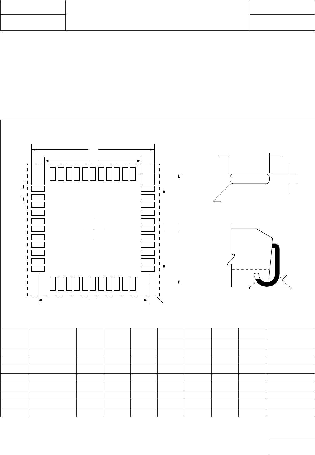
5.0 LAND PATTERN DIMENSIONS
Figure 3 provides the land pattern dimensions for PLCC
(Square) components. These numbers represent industry
consensus on the best dimensions based on empirical knowl-
edge of fabricated land patterns.
In the table, the dimensions shown are at maximum material
condition (MMC). The least material condition (LMC) should
not exceed the fabrication (F) allowance shown on page 4.
The LMC and the MMC provide the limits for each dimension.
The dotted line in Figure 3 shows the grid placement court-
yard which is the area required to place land patterns and
their respective components in adjacent proximity without
interference or shorting. Numbers in the table represent the
number of grid elements (each element is 0.5 by 0.5 mm) in
accordance with the international grid detailed in IEC publica-
tion 97.
RLP No.
Component
Identifier Z (mm) G (mm) X (mm)
Y (mm) C (mm) D (mm) E (mm)
Placement Grid
(No. of Grid
Elements)ref ref ref ref
790A PLCC-20 10.80 6.40 0.60 2.20 8.60 5.08 1.27 24x24
791A PLCC-28 13.40 9.00 0.60 2.20 11.20 7.62 1.27 30x30
792A PLCC-44 18.40 14.00 0.60 2.20 16.20 12.70 1.27 40x40
793A PLCC-52 21.00 16.60 0.60 2.20 18.80 15.24 1.27 44x44
794A PLCC-68 26.00 21.60 0.60 2.20 23.80 20.32 1.27 54x54
795A PLCC-84 31.20 26.80 0.60 2.20 29.00 25.40 1.27 66x66
796A PLCC-100 36.20 31.80 0.60 2.20 34.00 30.48 1.27 76x76
797A PLCC-124 43.80 39.40 0.60 2.20 41.60 38.10 1.27 90x90
Figure 3 PLCC (Square) land pattern dimensions
Z
G
D
C
Full radius
optional
▼
▼
▼
▼
▼
E
▼
Heel
Y
X
▼
Grid placement
courtyard
C
IPC-782-12-1-3
IPC-SM-782
Subject
PLCC (Square)
Date
5/96
Section
12.1
Revision
A
Page3of4
电子技术应用 www.ChinaAET.com