IPC-SM-782A 表面安装设计和焊盘设计标准(带BGA).pdf - 第185页
1.0 INTRODUCTION This section covers land patterns for DIPs (Modified Dual-In- Line components). Each subsection contains information in accordance with the following format: 1.0 Scope 2.0 Applicable Documents 3.0 Genera…
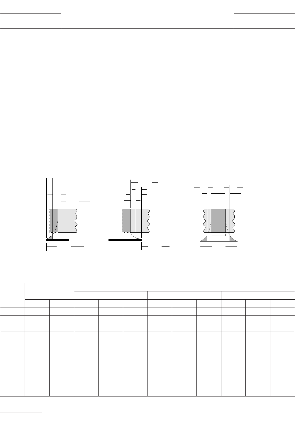
6.0 TOLERANCE AND SOLDER JOINT ANALYSIS
Figure 4 provides an analysis of tolerance assumptions and
resultant solder joints based on the land pattern dimensions
shown in Figure 3. Tolerances for the component dimensions,
the land pattern dimensions (fabrication tolerances on the
interconnecting substrate), and the component placement
equipment accuracy are all taken into consideration.
Figure 4 provides the solder joint minimums for toe, heel, and
side fillets, as discussed in Section 3.3. The tolerances are
addressed in a statistical mode, and assume even distribution
of the tolerances for component, fabrication, and placement
accuracy.
Individual tolerances for fabrication (‘‘F’’) and component
placement equipment accuracy (‘‘P’’) are assumed to be as
given in the table. These numbers may be modified based on
user equipment capability or fabrication criteria. Component
tolerance ranges (C
L
,C
S
, and C
W
) are derived by subtracting
minimum from maximum dimensions given in Figure 2. The
user may also modify these numbers, based on experience
with their suppliers. Modification of tolerances may result in
alternate land patterns (patterns with dimensions other than
the IPC registered land pattern dimensions).
The dimensions for minimum solder fillets at the toe, heel, or
side (J
T
,J
H
,J
S
) have been determined based on industry
empirical knowledge and reliability testing. Solder joint
strength is greatly determined by solder volume. An observ-
able solder fillet is necessary for evidence of proper wetting.
Thus, the values in the table usually provide for a positive sol-
der fillet. Nevertheless, the user may increase or decrease the
minimum value based on process capability.
RLP No.
Tolerance
Assumptions (mm)
Solder Joint
Toe (mm) Heel (mm) Side (mm)
FPC
L
J
T
min J
T
max C
S
J
H
min J
H
max C
W
J
S
min J
S
max
830 0.20 0.20 0.40 0.95 1.19 0.525 –0.02 0.28 0.480 –0.16 0.12
831 0.20 0.20 0.40 0.91 1.15 0.525 0.02 0.32 0.480 –0.16 0.12
832 0.20 0.20 0.37 0.95 1.18 0.502 –0.01 0.28 0.480 –0.16 0.12
833 0.20 0.20 0.40 0.94 1.18 0.525 –0.01 0.29 0.480 –0.16 0.12
834 0.20 0.20 0.50 0.98 1.27 0.604 –0.09 0.24 0.480 –0.16 0.12
835 0.20 0.20 0.54 0.91 1.21 0.638 -0.03 0.32 0.480 –0.16 0.12
836 0.20 0.20 0.60 0.85 1.19 0.689 –0.00 0.37 0.480 –0.16 0.12
837 0.20 0.20 0.76 0.88 1.28 0.832 –0.10 0.34 0.480 –0.16 0.12
838 0.20 0.20 0.54 0.89 1.19 0.638 –0.01 0.34 0.480 –0.16 0.12
839 0.20 0.20 0.54 0.98 1.28 0.638 –0.10 0.25 0.480 –0.16 0.12
840 0.20 0.20 0.54 0.90 1.20 0.638 –0.02 0.33 0.480 –0.16 0.12
Figure 4 Tolerance and solder joint analysis
Lmin
▼
▼
Zmax
▼
▼
1
/2 T
T
J
T
min
Zmax = Lmin + 2J
T
min + T
T
Where:
J
T
min = Minimum toe fillet
T
T
= Combined tolerances
at toe fillet
Gmin = Smax - 2J
H
min - T
H
Where:
J
H
min = Minimum heel fillet
T
H
= Combined tolerances
at heel fillet
Xmax = Wmin + 2J
S
min + T
S
Where:
J
S
min = Minimum side fillet
T
S
= Combined tolerances
at side fillet
Toe Fillet
▼
▼
▼
Heel Fillet Side Fillet
▼
▼
▼
▼
▼
J
T
max
▼
▼
▼
Gmin
Xmax
▼
▼
1
/2 T
S
J
S
max
▼
▼
▼
▼
▼▼
▼
J
S
min
Wmin
▼
▼
▼
▼
▼▼
▼
J
S
min
J
S
max
Smax
J
H
min
1
/2 T
H
J
H
max
▼
▼
▼
▼
▼
▼
▼
▼
▼
IPC-782-12-3-4
IPC-SM-782
Subject
LCC
Date
8/93
Section
12.3
Revision
Page4of4
电子技术应用 www.ChinaAET.com

1.0 INTRODUCTION
This section covers land patterns for DIPs (Modified Dual-In-
Line components). Each subsection contains information in
accordance with the following format:
1.0 Scope
2.0 Applicable Documents
3.0 General Component Description (Figure 1)
4.0 Component Dimensions (Figure 2)
5.0 Land Pattern Dimensions (Figure 3)
6.0 Tolerance and Solder Joint Analysis (Figure 4)
The following is the table of contents for this section:
Table of Contents
Modified Dual-In-Line Components
Section Component Standard Source
13.1 DIP JEDEC Publication 95
2.0 APPLICABLE DOCUMENTS
The following documents, of the issue in effect on the revision
date of this section, form a part of this specification to the
extent specified herein.
2.1 Electronic Industries Association (EIA)
1
EIA-481-A
Taping of Surface Mount Components for Auto-
matic Placement
EIA-481-2
16 mm and 24 mm Embossed Carrier Taping of
Surface Mount Components for Automated Handling
EIA-481-3
32 mm, 44 mm, and 56 mm Embossed Carrier
Taping of Surface Mount Components for Automated Han-
dling
JEDEC Publication
Registered and Standard Outlines for
Solid State and Related Products:
Outline Issue Title
MS-001 C Standard Dual-In-Line Family, 0.300
in. Row Spacing (Plastic)
MS-010 B Standard Dual-In-Line Family, 0.400
in. Row Spacing (Plastic)
MS-011 B Standard Dual-In-Line Family, 0.600
in. Row Spacing (Plastic)
2.2 International Electrotechnical Commission (IEC)
2
IEC 97
Grid Elements
3.0 GENERAL INFORMATION
3.1 General Component Description
A method of modi-
fying DIPs for surface mounting is the ‘‘I’’ mounting technique.
This involves simply cutting the DIP leads to a short length and
placing the device on a pattern of lands to be soldered along
with the other surface mounted devices.
1. Application for copies should be addressed to Global Engi-
neering Documents, 1990 M St. N.W., Washington, DC
20036.
2. Application for copes should be addressed to IEC, 3 rue
de Varembe, PO Box 131 - 1211 Geneva 20, Switzerland
IPC-SM-782
Surface Mount Design
and Land Pattern Standard
Date
8/93
Section
13.0
Revision Subject
DIPs
Page1of2
电子技术应用 www.ChinaAET.com

Page Intentionally Left Blank
IPC-SM-782
Subject
DIPs
Date
8/93
Section
13.0
Revision
Page2of2
电子技术应用 www.ChinaAET.com