IPC-SM-782A 表面安装设计和焊盘设计标准(带BGA).pdf - 第187页
1.0 SCOPE This subsection provides the component and land pattern dimensions for DIPs (Modified Dual-In-Line components). Basic construction of the DIP device is also covered. At the end of this subsection is a listing o…

Page Intentionally Left Blank
IPC-SM-782
Subject
DIPs
Date
8/93
Section
13.0
Revision
Page2of2
电子技术应用 www.ChinaAET.com
1.0 SCOPE
This subsection provides the component and land pattern
dimensions for DIPs (Modified Dual-In-Line components).
Basic construction of the DIP device is also covered. At the
end of this subsection is a listing of the tolerances and target
solder joint dimensions used to arrive at the land pattern
dimensions.
2.0 APPLICABLE DOCUMENTS
See Section 13.0 for documents applicable to the subsec-
tions.
3.0 COMPONENT DESCRIPTIONS
3.1 Basic Construction
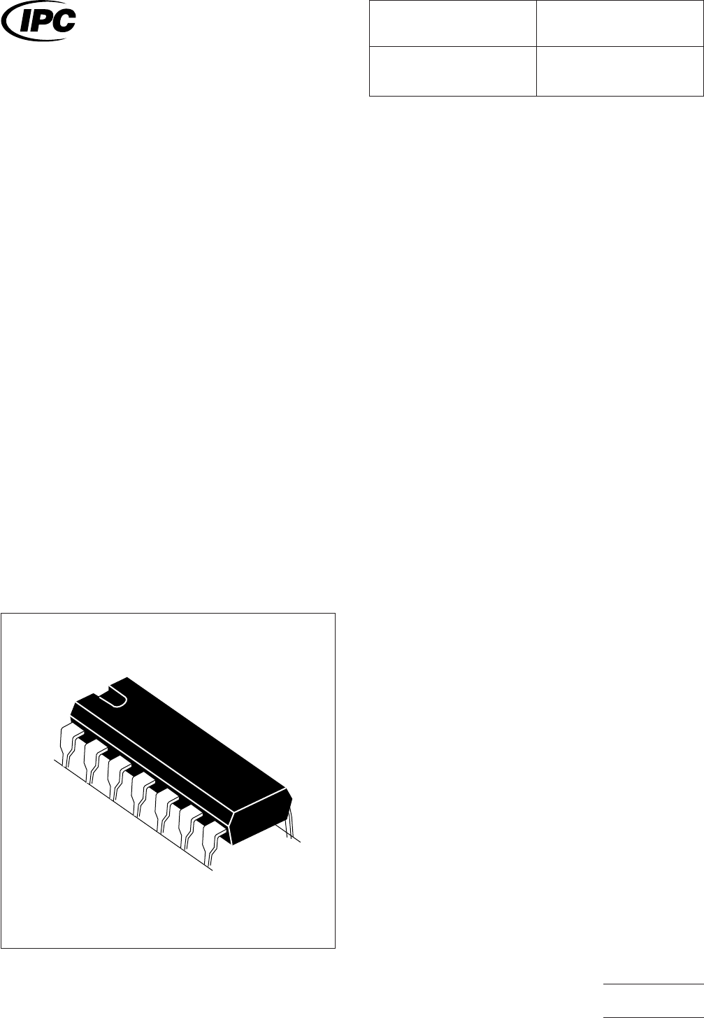
See Figure 1. Construction is usu-
ally made of plastic or ceramics.
3.1.1 Termination Materials
Leads should be solder-
coated with a tin/lead alloy. The solder should contain
between 58 to 68% tin. Solder may be applied to the termi-
nation by hot dipping or by plating from solution. Plated sol-
der terminations should be subjected to a post-plating reflow
operation to fuse the solder. The tin/lead finish should be at
least 0.00075 mm [0.0003 in] thick.
Solder finish applied over precious-metal leads shall have a
diffusion-barrier layer between the lead metallization and the
solder finish. The barrier layer should be nickel or an equiva-
lent diffusion barrier, and should be at least 0.00125 mm
[0.00005 in] thick.
3.1.2 Marking
Parts shall be marked with the part number
and a date code. In addition, pin 1 shall be identified.
3.1.3 Carrier Package Format
Carrier format may be
tubes or as agreed to between user and vendor.
3.1.4 Resistance to Soldering
The parts should be
capable of withstanding ten cycles through a standard reflow
system operating at 215°C. Each cycle shall consist of a mini-
mum of 60 seconds exposure at 215°C.
IPC-782-13-1-1
Figure 1 DIP construction
IPC-SM-782
Surface Mount Design
and Land Pattern Standard
Date
8/93
Section
13.1
Revision Subject
DIP
Page1of4
电子技术应用 www.ChinaAET.com
IPC-782-13-1-2
A
▼
▼
B
▼
▼
H
▼
▼ ▼
▼
.38
▼
▼
D
W
P
▼
▼
▼
▼
L
▼
▼
▼
▼
T
W
.25
▼
▼
▼
▼
▼
Cut line
S
▼
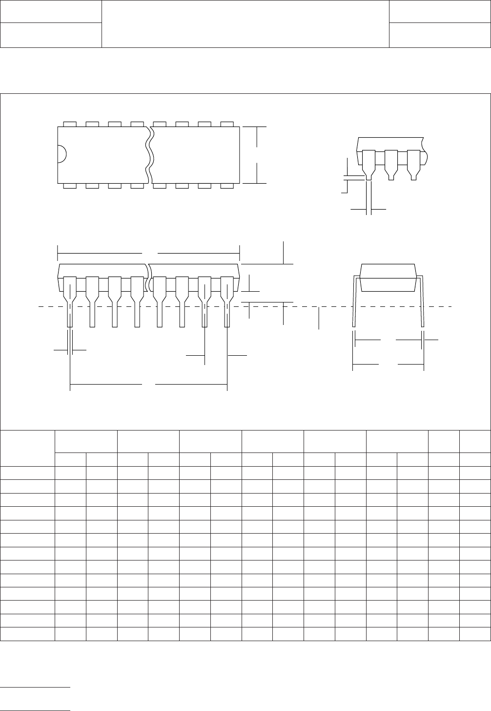
4.0 COMPONENT DIMENSIONS
Figure 2 provides the component dimensions for DIP components.
Component
Identifier
L (mm) S (mm) W (mm) T (mm) A (mm) B (mm)
H
(mm)
P
(mm)
min max min max min max min max m in max min max max basic
DIP 8 7.62 8.25 6.86 7.54 0.36 0.56 0.20 0.38 6.10 7.11 8.84 10.92 5.33 2.54
DIP 14 7.62 8.25 6.86 7.54 0.36 0.56 0.20 0.38 6.10 7.11 18.42 20.19 5.33 2.54
DIP 16 7.62 8.25 6.86 7.54 0.36 0.56 0.20 0.38 6.10 7.11 18.93 21.33 5.33 2.54
DIP 18 7.62 8.25 6.86 7.54 0.36 0.56 0.20 0.38 6.10 7.11 21.47 23.49 5.33 2.54
DIP 20 7.62 8.25 6.86 7.54 0.36 0.56 0.20 0.38 6.10 7.11 23.50 26.90 5.33 2.54
DIP 22L 9.91 10.79 9.15 10.07 0.36 0.56 0.20 0.38 8.39 9.65 26.67 28.44 5.33 2.54
DIP 24 7.62 8.25 6.86 7.54 0.36 0.56 0.20 0.38 6.10 7.11 28.60 32.30 5.33 2.54
DIP 24L 9.91 10.79 9.15 10.07 0.36 0.56 0.20 0.38 8.39 9.65 29.21 30.98 5.33 2.54
DIP 24X 15.24 15.87 14.48 15.16 0.36 0.56 0.20 0.38 12.32 14.73 29.30 32.70 6.35 2.54
DIP 28 7.62 8.25 6.86 7.54 0.36 0.56 0.20 0.38 6.10 7.11 34.20 36.20 5.33 2.54
DIP 28X 15.24 15.87 14.48 15.16 0.36 0.56 0.20 0.38 12.32 14.73 35.10 39.70 6.35 2.54
DIP 40X 15.24 15.87 14.48 15.16 0.36 0.56 0.20 0.38 12.32 14.73 50.30 53.20 6.35 2.54
DIP 48X 15.24 15.87 14.48 15.16 0.36 0.56 0.20 0.38 12.32 14.73 60.70 63.10 6.35 2.54
Figure 2 DIP component dimensions
IPC-SM-782
Subject
DIP
Date
8/93
Section
13.1
Revision
Page2of4
电子技术应用 www.ChinaAET.com