IPC-SM-782A 表面安装设计和焊盘设计标准(带BGA).pdf - 第189页
5.0 LAND PATTERN DIMENSIONS Figure 3 provides the land pattern dimensions for DIP compo- nents. These numbers represent industry consensus on the best dimensions based on empirical knowledge of fabricated land patterns. …
IPC-782-13-1-2
A
▼
▼
B
▼
▼
H
▼
▼ ▼
▼
.38
▼
▼
D
W
P
▼
▼
▼
▼
L
▼
▼
▼
▼
T
W
.25
▼
▼
▼
▼
▼
Cut line
S
▼
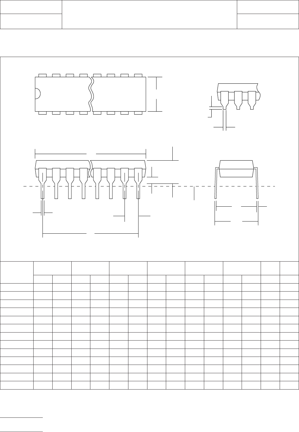
4.0 COMPONENT DIMENSIONS
Figure 2 provides the component dimensions for DIP components.
Component
Identifier
L (mm) S (mm) W (mm) T (mm) A (mm) B (mm)
H
(mm)
P
(mm)
min max min max min max min max m in max min max max basic
DIP 8 7.62 8.25 6.86 7.54 0.36 0.56 0.20 0.38 6.10 7.11 8.84 10.92 5.33 2.54
DIP 14 7.62 8.25 6.86 7.54 0.36 0.56 0.20 0.38 6.10 7.11 18.42 20.19 5.33 2.54
DIP 16 7.62 8.25 6.86 7.54 0.36 0.56 0.20 0.38 6.10 7.11 18.93 21.33 5.33 2.54
DIP 18 7.62 8.25 6.86 7.54 0.36 0.56 0.20 0.38 6.10 7.11 21.47 23.49 5.33 2.54
DIP 20 7.62 8.25 6.86 7.54 0.36 0.56 0.20 0.38 6.10 7.11 23.50 26.90 5.33 2.54
DIP 22L 9.91 10.79 9.15 10.07 0.36 0.56 0.20 0.38 8.39 9.65 26.67 28.44 5.33 2.54
DIP 24 7.62 8.25 6.86 7.54 0.36 0.56 0.20 0.38 6.10 7.11 28.60 32.30 5.33 2.54
DIP 24L 9.91 10.79 9.15 10.07 0.36 0.56 0.20 0.38 8.39 9.65 29.21 30.98 5.33 2.54
DIP 24X 15.24 15.87 14.48 15.16 0.36 0.56 0.20 0.38 12.32 14.73 29.30 32.70 6.35 2.54
DIP 28 7.62 8.25 6.86 7.54 0.36 0.56 0.20 0.38 6.10 7.11 34.20 36.20 5.33 2.54
DIP 28X 15.24 15.87 14.48 15.16 0.36 0.56 0.20 0.38 12.32 14.73 35.10 39.70 6.35 2.54
DIP 40X 15.24 15.87 14.48 15.16 0.36 0.56 0.20 0.38 12.32 14.73 50.30 53.20 6.35 2.54
DIP 48X 15.24 15.87 14.48 15.16 0.36 0.56 0.20 0.38 12.32 14.73 60.70 63.10 6.35 2.54
Figure 2 DIP component dimensions
IPC-SM-782
Subject
DIP
Date
8/93
Section
13.1
Revision
Page2of4
电子技术应用 www.ChinaAET.com
5.0 LAND PATTERN DIMENSIONS
Figure 3 provides the land pattern dimensions for DIP compo-
nents. These numbers represent industry consensus on the
best dimensions based on empirical knowledge of fabricated
land patterns.
In the table, the dimensions shown are at maximum material
condition (MMC). The least material condition (LMC) should
not exceed the fabrication (F) allowance shown on page 4.
The LMC and the MMC provide the limits for each dimension.
The dotted line in Figure 3 shows the grid placement court-
yard which is the area required to place land patterns and
their respective components in adjacent proximity without
interference or shorting. Numbers in the table represent the
number of grid elements (each element is 0.5 by 0.5 mm) in
accordance with the international grid detailed in IEC publica-
tion 97.
RLP No.
Component
Identifier Z (mm) G (mm) X (mm)
Y (mm) C (mm) D (mm) E (mm)
Placement Grid
(No. of Grid
Elements)ref ref ref ref
860 DIP 8 9.80 5.40 1.20 2.20 7.60 7.62 2.54 22x24
861 DIP 14 9.80 5.40 1.20 2.20 7.60 15.24 2.54 22x42
862 DIP 16 9.80 5.40 1.20 2.20 7.60 17.78 2.54 22x44
863 DIP 18 9.80 5.40 1.20 2.20 7.60 20.32 2.54 22x48
864 DIP 20 9.80 5.40 1.20 2.20 7.60 22.86 2.54 22x56
865 DIP 22L 12.40 8.00 1.20 2.20 10.20 25.40 2.54 26x58
866 DIP 24 9.80 5.40 1.20 2.20 7.60 27.94 2.54 38x66
867 DIP 24L 12.40 8.00 1.20 2.20 10.20 27.94 2.54 26x64
867 DIP 24X 17.40 13.00 1.20 2.20 15.20 27.94 2.54 36x68
869 DIP 28 9.80 5.40 1.20 2.20 7.60 33.02 2.54 22x74
870 DIP 28X 17.40 13.00 1.20 2.20 15.20 33.02 2.54 36x84
871 DIP 40X 17.40 13.00 1.20 2.20 15.20 48.26 2.54 36x110
872 DIP 48X 17.40 13.00 1.20 2.20 15.20 58.42 2.54 36x130
Figure 3 DIP land pattern dimensions
IPC-782-13-1-3
IPC-SM-782
Subject
DIP
Date
8/93
Section
13.1
Revision
Page3of4
电子技术应用 www.ChinaAET.com
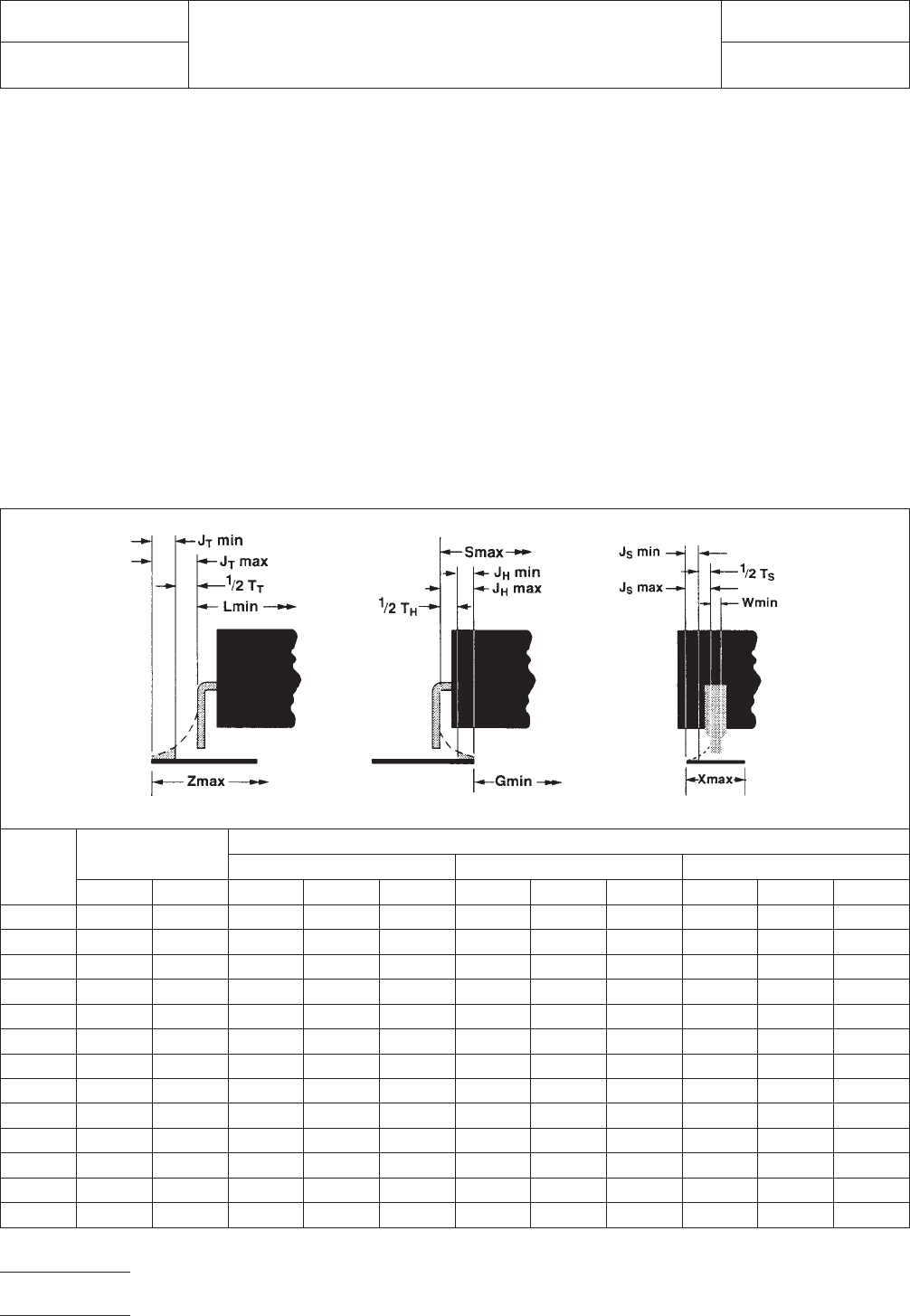
6.0 TOLERANCE AND SOLDER JOINT ANALYSIS
Figure 4 provides an analysis of tolerance assumptions and
resultant solder joints based on the land pattern dimensions
shown in Figure 3. Tolerances for the component dimensions,
the land pattern dimensions (fabrication tolerances on the
interconnecting substrate), and the component placement
equipment accuracy are all taken into consideration.
Figure 4 provides the solder joint minimums for toe, heel, and
side fillets, as discussed in Section 3.3. The tolerances are
addressed in a statistical mode, and assume even distribution
of the tolerances for component, fabrication, and placement
accuracy.
Individual tolerances for fabrication (‘‘F’’) and component
placement equipment accuracy (‘‘P’’) are assumed to be as
given in the table. These numbers may be modified based on
user equipment capability or fabrication criteria. Component
tolerance ranges (C
L
,C
S
, and C
W
) are derived by subtracting
minimum from maximum dimensions given in Figure 2. The
user may also modify these numbers, based on experience
with their suppliers. Modification of tolerances may result in
alternate land patterns (patterns with dimensions other than
the IPC registered land pattern dimensions).
The dimensions for minimum solder fillets at the toe, heel, or
side (J
T
,J
H
,J
S
) have been determined based on industry
empirical knowledge and reliability testing. Solder joint
strength is greatly determined by solder volume. An observ-
able solder fillet is necessary for evidence of proper wetting.
Thus, the values in the table usually provide for a positive sol-
der fillet. Nevertheless, the user may increase or decrease the
minimum value based on process capability.
RLP No.
Tolerance
Assumptions (mm)
Solder Joint
Toe (mm) Heel (mm) Side (mm)
FPC
L
J
T
min J
T
max C
S
J
H
min J
H
max C
W
J
S
min J
S
max
860 0.20 0.20 0.630 0.74 1.09 0.679 0.70 1.07 0.200 0.25 0.42
861 0.20 0.20 0.630 0.74 1.09 0.679 0.70 1.07 0.200 0.25 0.42
862 0.20 0.20 0.630 0.74 1.09 0.679 0.70 1.07 0.200 0.25 0.42
863 0.20 0.20 0.630 0.74 1.09 0.679 0.70 1.07 0.200 0.25 0.42
864 0.20 0.20 0.630 0.74 1.09 0.679 0.70 1.07 0.200 0.25 0.42
865 0.20 0.20 0.880 0.78 1.25 0.916 0.55 1.03 0.200 0.25 0.42
866 0.20 0.20 0.630 0.74 1.09 0.679 0.70 1.07 0.200 0.25 0.42
867 0.20 0.20 0.880 0.78 1.25 0.916 0.55 1.03 0.200 0.25 0.42
868 0.20 0.20 0.630 0.73 1.08 0.679 0.71 1.08 0.200 0.25 0.42
869 0.20 0.20 0.630 0.74 1.09 0.679 0.70 1.07 0.200 0.25 0.42
870 0.20 0.20 0.630 0.73 1.08 0.679 0.71 1.08 0.200 0.25 0.42
871 0.20 0.20 0.630 0.73 1.08 0.679 0.71 1.08 0.200 0.25 0.42
872 0.20 0.20 0.630 0.73 1.08 0.679 0.71 1.08 0.200 0.25 0.42
Figure 4 Tolerance and solder joint analysis
IPC-782-13-1-4
IPC-SM-782
Subject
DIP
Date
8/93
Section
13.1
Revision
Page4of4
电子技术应用 www.ChinaAET.com