IPC-SM-782A 表面安装设计和焊盘设计标准(带BGA).pdf - 第196页
This Page Intentionally Left Blank IPC-SM-782A Subject Components with Ball Grid Array Contacts Date 4/99 Section 14.0 Revision — P a g e6o f6 电子技术应用 www.ChinaAET.com
by taking the maximum land size and subtracting the varia-
tion. The resulting dimension would indicate the amount of
attachment area that would result from a system where all
conditions are at a negative instance. For lands that are sol-
der mask-defined, the land size should be increased by the
amount of encroachment of the solder mask. As an example,
if the requirement is that solder mask should be on the land
by 0.05 mm, then the maximum land size should be increased
by 0.1. It should be noted that for solder mask-defined lands,
since the land size increases, the opportunity to route con-
ductors between lands is impacted by reducing the available
area for conductor width and spacing.
6.3 Future Ball Conditions Although not required for the
BGAs shown in the present release of 14.0, future ball sizes
contemplated are shown in Table 6-1. Their land size approxi-
mations are shown in Table 6-2.
6.4 Land Pattern Calculator
The land pattern calcula-
tions for BGAs are based on ball size. As a result of ball varia-
tion and component conditions, Table 6-4 shows the land
pattern calculator headings needed to describe the variations
in the system. The RLP number pertains to a single land. It is
applicable to all the registered land pattern numbers for the
various registered packages shown in Section 14. This data is
usually described at the Maximum Material Condition for non-
solder mask-defined lands and is dimension X in the various
sections. The registered single land pattern numbers for the
various ball sizes are shown in Table 6-4.
Table 6-4 Land-to-Ball Calculations for Current and Future BGA Packages (mm)
RLP
Land Size
Location
Allowance
Ball
Variation
PCB
Fabrication
Allowance
Ball Size
%
Reduction
From Nom.
Variation
AllowanceMMC LMC Nominal MMC LMC
050 0.60 0.50 0.10 0.25 0.10 0.75 0.90 0.65 25% 0.25
051 0.50 0.40 0.10 0.20 0.10 0.60 0.70 0.50 25% 0.20
052 0.45 0.35 0.10 0.10 0.10 0.50 0.55 0.45 20% 0.17
053 0.40 0.30 0.10 0.10 0.10 0.45 0.50 0.40 20% 0.17
054 0.35 0.25 0.10 0.10 0.10 0.40 0.45 0.35 20% 0.17
055 0.25 0.20 0.05 0.10 0.05 0.30 0.35 0.25 20% 0.15
056 0.20 0.17 0.05 0.06 0.03 0.25 0.28 0.22 20% 0.08
057 0.15 0.12 0.05 0.04 0.03 0.20 0.22 0.18 20% 0.07
058 0.10 0.08 0.05 0.04 0.02 0.15 0.17 0.13 20% 0.07
Table 6-2 Land Approximation
Nominal Ball
Diameter
(mm) Reduction
Nominal
Land
Diameter
(mm)
Land
Variation
(mm)
0.75 25% 0.55 0.60 - 0.50
0.60 25% 0.45 0.50 - 0.40
0.50 20% 0.40 0.45 - 0.35
0.45 20% 0.35 0.40 - 0.30
0.40 20% 0.30 0.35 - 0.25
0.30 20% 0.25 0.25 - 0.20
0.25 20% 0.20 0.20 - 0.17
0.20 20% 0.15 0.15 - 0.12
0.15 20% 0.10 0.10 - 0.08
Table 6-3 BGA Variation Attributes
Nominal
Ball
Size
(mm)
Positional
Allowance
Ball
Tolerance
(mm)
Substrate
Tolerance
(mm)
Variation
RMS
Value
0.75 0.1 dia. DTP 0.25 0.10 0.25
0.60 0.1 dia. DTP 0.20 0.10 0.24
0.50 0.1 dia. DTP 0.10 0.10 0.17
0.45 0.1 dia. DTP 0.10 0.10 0.17
IPC-SM-782A
Subject
Components with Ball Grid Array Contacts
Date
4/99
Section
14.0
Revision
—
Page5of6
电子技术应用 www.ChinaAET.com

This Page Intentionally Left Blank
IPC-SM-782A
Subject
Components with Ball Grid Array Contacts
Date
4/99
Section
14.0
Revision
—
Page6of6
电子技术应用 www.ChinaAET.com
1.0 INTRODUCTION
This section covers land pattern recommendations for ball
grid array (BGA) contact devices. Each subsection contains
information in accordance with the following format.
1.0 Scope
2.0 Applicable Documents
3.0 General Component Description
4.0 Component Outline
5.0 Land Pattern Dimensions
6.0 Land Pattern Analysis
The following is the table of contents for this section:
Table of Contents
Components with Ball Grid Array Contacts
Section
14.1.1
14.1.2
14.1.3
Standard Source
JEDEC MO-151
JEDEC MO-151
JEDEC MO-151
Pitch
1.5 mm
1.27 mm
1.0 mm
2.0 APPLICABLE DOCUMENTS
The following documents, of the issue in effect on the current
revision date of this section, form a part of this specification to
the extent specified herein.
2.1 Joint Electronic Device Engineering Council
1
JEDEC Publication 95
Registered and Standard Outlines for
Solid State and Related Products:
• Plastic Ball Grid Array (PBGA), MO-151
3.0 GENERAL INFORMATION
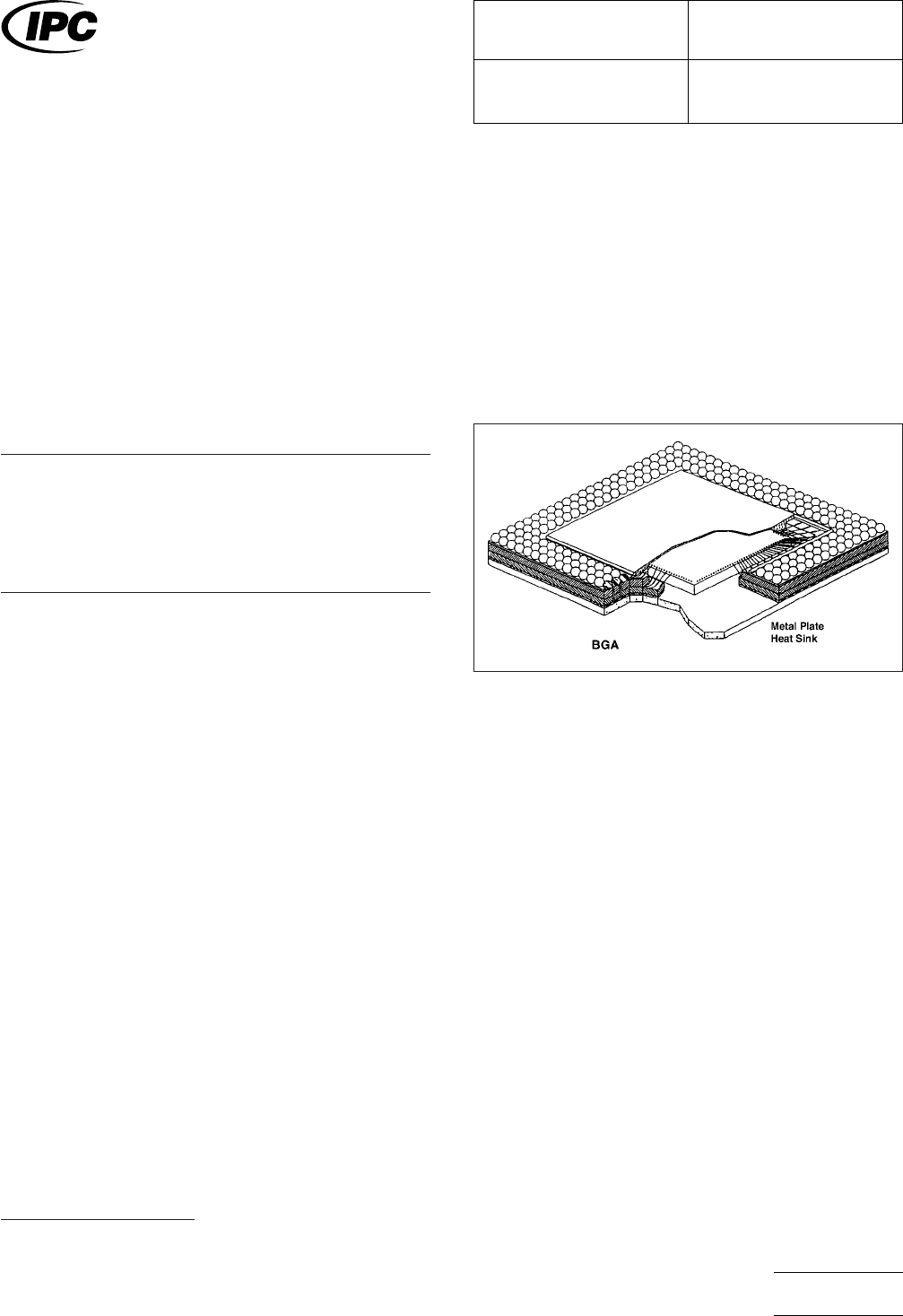
3.1 Component Description
The Grid Array device family
includes square and rectangular package configurations and
is furnished in a plastic base material. Figure 3-1 shows the
elements of a BGA. Base material serves as a mounting struc-
ture for attaching the die. Depending on the physical charac-
teristics of the material, flip-chip or wire bond technologies
may be employed to route the signal from the die bond pads
to the array matrix on the base interface structure.
1. JEDEC: 2500 Wilson Blvd., Arlington, VA, 22201-3834, USA.
IPC-782143-1
Figure 3-1 Ball Grid Array IC package example
IPC-SM-782
Surface Mount Design
and Land Pattern Standard
Date
4/99
Section
14.1
Revision
—
Subject
Plastic Ball Grid Array
Page1of2
电子技术应用 www.ChinaAET.com