IPC-SM-782A 表面安装设计和焊盘设计标准(带BGA).pdf - 第222页
• Zone 3 Zone 3 is where the information must be entered for describing the relationship of the component dimensions to be used in the analysis. See Figure A-2. • Zone 4 Zone 4 represents the manufacturing allowance. Thi…

Appendix A
IPC-EM-782
Data Analysis Spreadsheets
for IPC-SM-782 Land Patterns
The IPC has developed a spreadsheet and user’s guide for
the manipulation of data that supports the concepts and
methodology for developing surface mount land patterns
that are identified in IPC-SM-782, ‘‘Surface Mount Design
and Land Pattern Standard.’’ This product is:
IPC-EM-782, ‘‘Data Analysis Spreadsheets for IPC-SM-
782 Land Patterns’’
The information contained in the various files of the disk
provide the appropriate size, shape, and tolerance of sur-
face mount land patterns that insure sufficient area for
appropriate solder fillets, and allow for the inspection and
testing of those solder joints.
The equations built into the spreadsheet format follow the
principles delineated in IPC-SM-782. They have been orga-
nized into various columns and rows for ease of use in both
understanding the principles, and allowing users of the disk
to manipulate the data in a manner to achieve optimum
solder joint formation for their particular projects.
The data reflects the printed and agreed to land pattern
sizes. Each land pattern has been registered with its own
number in a significant numbering system that correlates a
land pattern to a specific surface mount component.
Although many spreadsheets exist in industry, Lotus was
chosen because these concepts were relatively basic, and
could be used by the majority of other spreadsheet pro-
grams. Although newer and more exotic techniques are
available, the principles embodied in the ‘‘Electronic
Media (EM)‘‘ have been kept as simple as possible so that
the information can be transported to other spreadsheets
with which users feel more comfortable.
Names of Files
There are numerous files on the master disc. They match
the component families and their assigned section.
The following is an example of the names of the files and
their descriptions related to the IPC-SM-782:
8.1 Chip Resistors 81CHPRES.WK1
8.2 Chip Depositors 82CHPCAP.WK1
8.3 Inductors 83CHPIND.WK1
8.4 Teflon Capacitors 84DANCAP.WK1
8.5 Metal Electrode Face (Components) 85MELS.WK1
8.6 Small Outline Transistor(SOD) 23 86SOD23.WK1
8.7 Small Outline Transistor (SOD) 89 87SOD89.WK1
8.8 Small Outline Diode (SOD) 123 88SOD123.WK1
8.9 Small Outline Transistors (SOD)143 89SOD143.WK1
8.10 Small Outline Transistors (SOD) 810SO223.WK1
IPC-EM-782 (Users Guide and 3 1/2 Disc) is available
from IPC:
$50.00 for IPC members, $100.00 for nonmembers
Spreadsheet Zones
Each spreadsheet has been divided into 10 zones. Each of
these zones serves a specific function, and is intended to
help the user work through the details of the particular pro-
gram analysis in which he wishes to accomplish the design
of a land pattern. The following is the description and pur-
pose of each of the zones, using the chip resistor file 81
CHPRES. WK1 as the model.
• Zone 1
Zone 1 provides the registered land pattern number in
column B, and the component identification in metric in
column C. It is always a good idea to fix this zone in
place, so that the information is always displayed as the
user is moving back and forth along the file. See Figure
A-1.
• Zone 2
Zone 2 is intended to describe the finished land pattern
dimension. These include the Z maximum dimension; the
G minimum dimension; the X maximum dimension; and
a reference for the Y dimension, which is derived by sub-
tracting G from Z and dividing by 2. The center point of
the two land patterns, and a good placement courtyard
area, are intended to encompass the respective compo-
nents without interference or shorting. The numbers in the
table represent the number of grade elements (each ele-
ment is 0.5 by 0.5 mm) in accordance with the interna-
tional grid detailed in IEC publication 97. See Figure A-1.
December 1999 IPC-SM-782A
A-1
电子技术应用 www.ChinaAET.com
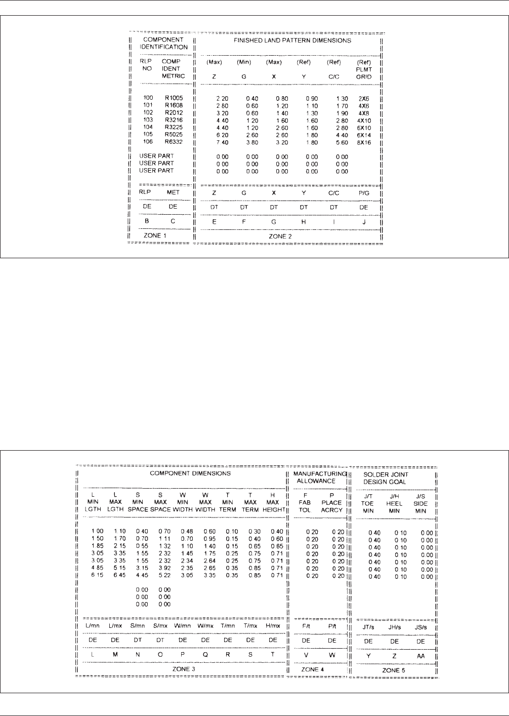
• Zone 3
Zone 3 is where the information must be entered for
describing the relationship of the component dimensions
to be used in the analysis. See Figure A-2.
• Zone 4
Zone 4 represents the manufacturing allowance. This
allowance is for the board manufacturing tolerance, and
for placement accuracy, and is contained in columns V
and W of the spreadsheet for chip resistors. See Figure
A-2.
• Zone 5
Zone 5 represents the solder joint design goal informa-
tion. This information is entered by the user, and reflects
the desired solder joint at the toe, heel and side.
The recommendations come from empirical information
that has been determined over the years for the derivation
of process proven land patterns. See Figure A-2.
Figure A-1 Zones 1 and 2
Figure A-2 Zones 3, 4, and 5
IPC-SM-782A December 1999
A-2
电子技术应用 www.ChinaAET.com
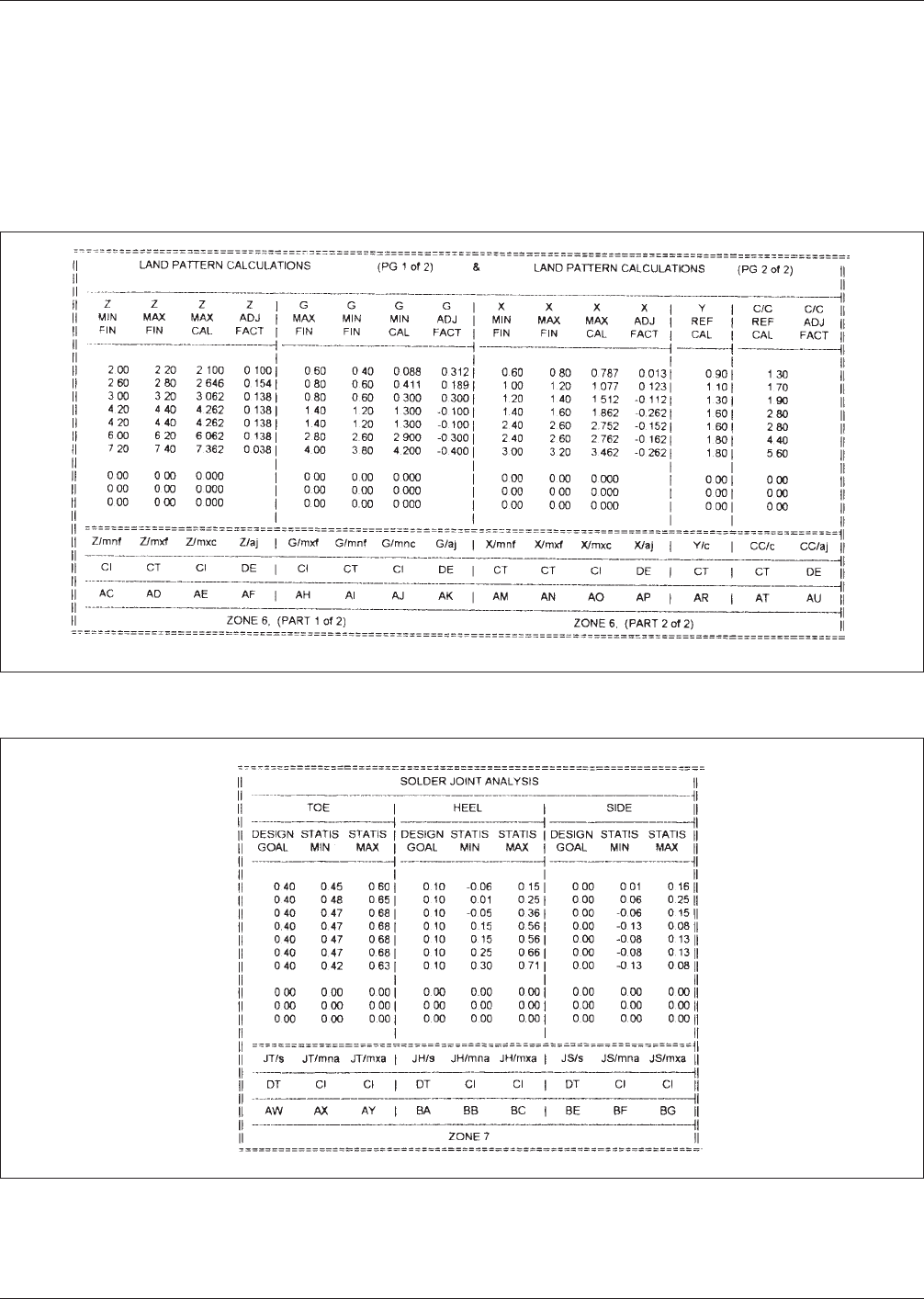
• Zone 6
Zone 6 is the most important part of the analysis. It is in
this area where the user has the opportunity to fine tune
the land pattern through the adjustment factor to enhance
the pattern for both solder joint formation and character-
istics that can be used by the CAD systems. See Figure
A-3.
• Zone 7
Zone 7 provides information as to what has been accom-
plished for the toe, heel, and side fillets. This zone is
divided into three segments. See Figure A-4.
Figure A-3 Zone 6
Figure A-4 Zone 7
December 1999 IPC-SM-782A
A-3
电子技术应用 www.ChinaAET.com